2-12
Service Guide
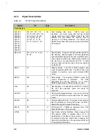
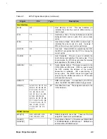
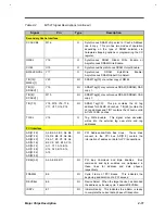
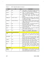
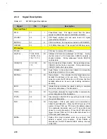
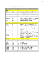
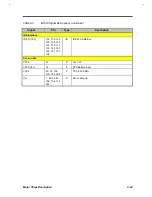
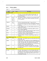
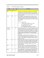
Table 2-2
M1521 Signal Descriptions (continued)
Signal
Pin
Type
Description
TRDYJ
E8
I/O
Target Ready. This indicates the target is ready to
complete the current data phase of transaction.
STOPJ
E11
I/O
Stop. This indicates the target is requesting the
master to stop the current transaction.
LOCKJ
E5
I/O
Lock Resource Signal. This indicates the PCI
master or the bridge intends to do exclusive
transfers.
REQJ[3:0]
D13, D11, D9, D7
I
Bus request signals of PCI Masters. When asserted,
it means the PCI master is requesting the PCI bus
ownership from the arbiter.
GNTJ[3:0]
D14, D12, D10, D8
O
Grant signals to PCI Masters. When asserted by the
arbiter, it means the PCI master has been legally
granted to own the bus.
PHLDJ
D4
I
PCI bus hold request. This active low signal is a
request from M1523 for the PCI bus.
PHLDAJ
D5
O
PCI bus hold acknowledge. This active low signal
grants PCI to M1523.
PAR
E12
I/O
Parity bit of PCI buses. It is the even parity bit
across PAD[31:0] and CBEJ[3:0].
SERRJ
E13
O
System Error. If the M1521 detects parity errors in
DRAMs, it asserts SERRJ to notify the system.
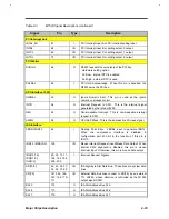
Clock, Reset, and Suspend Interfaces
RSTJ
T15
I
System Reset. This pin, when asserted, resets the
M1521 and sets the register bits to their default
values.
SUSPENDJ
P6
I
Suspend. When actively sampled, the M1521 enters
the I/O suspend mode. This signal should be pulled
high when the suspend feature is disabled.
HCLKIN
K16
I
CPU Bus Clock Input. This signal is used by all of
the M1521 logic that is in the host clock domain.
PCLKIN
E10
I
PCI Bus Clock Input. This signal is used by all of
the M1521 logic that is in the PCI clock domain.
32K
W17
I
The refresh reference clock of frequency 32khz
during suspend mode. This signal should be pulled
to a fixed value when the suspend feature is
disabled.
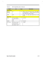
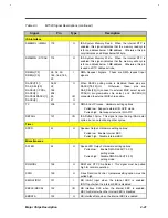
UMA Interface
MREQJ/
REQJ[4]
H6
I
Memory Request. This input signal is from the GUI
device’s MREQJ output. This pin can also be used
as bus request signal of the fifth PCI master.
Summary of Contents for AcerNote Light 370P
Page 6: ...vi ...
Page 26: ...1 8 Service Guide Figure 1 5 Main Board Layout Bottom Side ...
Page 49: ...System Introduction 1 31 1 5 1 3 Power Management Figure 1 14 Power Management Block Diagram ...
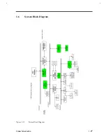
Page 55: ...System Introduction 1 37 1 6 System Block Diagram Figure 1 15 System Block Diagram ...
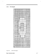
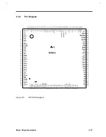
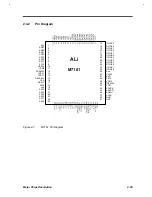
Page 64: ...Major Chips Description 2 7 2 2 5 Pin Diagram Figure 2 4 M1521 Pin Diagram ...
Page 99: ...2 42 Service Guide 2 5 3 Pin Diagram Figure 2 10 C T 65550 Pin Diagram ...
Page 117: ...2 60 Service Guide Figure 2 12 Functional block diagram CardBus Card Interface ...
Page 119: ...2 62 Service Guide Figure 2 14 PCI to CardBus terminal assignments ...
Page 135: ...2 78 Service Guide 2 7 3 Pin Diagram Figure 2 16 NS87336VJG Pin Diagram ...
Page 145: ...2 88 Service Guide 2 8 2 Pin Diagram Figure 2 17 YMF715 Block Diagram ...
Page 185: ...Disassembly and Unit Replacement 4 5 Figure 4 3 Disassembly Sequence Flowchart ...
Page 209: ...B 2 Service Guide ...
Page 210: ...Exploded View Diagram B 3 ...

