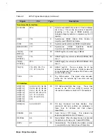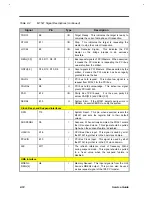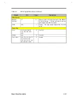
Major Chips Description
2-15
•
32-bit addressability
•
Provides compatible DMA transfers
•
Provides type F transfers
•
Interrupt controller
•
Provides 14 interrupt channels
•
Independently programmable level/edge triggered channels
•
Counter/Timers
•
Provides 8254 compatible timers for system timer, refresh request, speaker output use
•
Keyboard controller
•
Built-in PS2/AT keyboard controller
•
The specific I/O is used to save the external TTL buffer
•
Real time clock
•
Built-in real-time clock
•
128-byte CMOS RAM with 2µA standby current maximum
•
Plug-and-Play port support
•
programmable chip select
•
Steerable interrupt request lines
•
PMU interface
•
Supports CPU SMM mode, SMI feature
•
Supports programmable stop clock throttle
•
Supports the APM control
•
Provides external suspend mode switch/turbo switch/ring-in switch
•
Provides four system states for power saving (on, doze, standby, suspend)
•
Provides three timers from 1 second to 300 minutes to individually monitor VGA, MODE,
IN status
•
Supports RTC alarm wake up control
•
IDE interface
•
Built-in PCI IDE master controller
•
Supports PIO modes up to mode 5 timings, and multiword DMA mode 0, 1, 2
•
8 x 32-bit pre-read and posted-write buffers
•
Dedicated pins for ATA interface
•
Supports up to 256 KB ROM size decode
•
Reserved USB interface
•
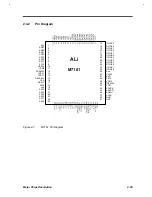
208-pin PQFP package
Summary of Contents for AcerNote Light 370P
Page 6: ...vi ...
Page 26: ...1 8 Service Guide Figure 1 5 Main Board Layout Bottom Side ...
Page 49: ...System Introduction 1 31 1 5 1 3 Power Management Figure 1 14 Power Management Block Diagram ...
Page 55: ...System Introduction 1 37 1 6 System Block Diagram Figure 1 15 System Block Diagram ...
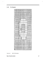
Page 64: ...Major Chips Description 2 7 2 2 5 Pin Diagram Figure 2 4 M1521 Pin Diagram ...
Page 99: ...2 42 Service Guide 2 5 3 Pin Diagram Figure 2 10 C T 65550 Pin Diagram ...
Page 117: ...2 60 Service Guide Figure 2 12 Functional block diagram CardBus Card Interface ...
Page 119: ...2 62 Service Guide Figure 2 14 PCI to CardBus terminal assignments ...
Page 135: ...2 78 Service Guide 2 7 3 Pin Diagram Figure 2 16 NS87336VJG Pin Diagram ...
Page 145: ...2 88 Service Guide 2 8 2 Pin Diagram Figure 2 17 YMF715 Block Diagram ...
Page 185: ...Disassembly and Unit Replacement 4 5 Figure 4 3 Disassembly Sequence Flowchart ...
Page 209: ...B 2 Service Guide ...
Page 210: ...Exploded View Diagram B 3 ...


