2-20
Service Guide
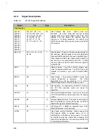
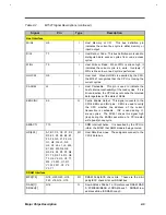
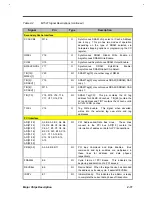
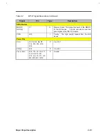
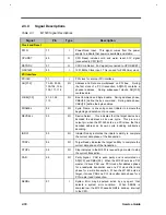
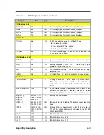
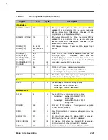
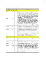
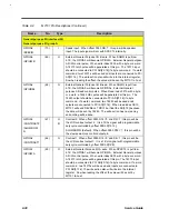
Table 2-3
M1523 Signal Descriptions (continued)
Signal
Pin
Type
Description
ISA Interface
SA[16:0]
181, 185, 187,
188, 190, 192,
193, 195, 197,
199, 201, 203,
205, 207, 3, 4,
5
I/O
ISA Slot Address Bus. These lines are addresses
connected to slot address.
SBHEJ
6
I/O
ISA Slot Byte-high Enable. In a CPU or PCI master cycle,
this signal is generated by BE3J-BE0J and the chip’s
internal control circuit. In a DMA cycle, it is generated by
internal 8237. In a refresh cycle, it is generated by the
internal refresh circuits. It is an input signal for ISA
master cycle.
LA[23:17]
8, 10, 12, 18,
19, 21, 23
I/O
ISA Latched Address Bus. They are input during ISA
master cycle.
IO16J
9
I
ISA 16-bit I/O Device Indicator. This signal indicates the
I/O device supports 16-bit transfers.
M16J
7
I/O
ISA 16-bit Memory Device Indicator. This signal indicates
the memory device supports 16-bit transfers.
MEMRJ
24
I/O
ISA Memory Read. This signal is an input during ISA
master cycle.
MEMWJ
27
I/O
ISA Memory Write. This signal is an input during ISA
master cycle.
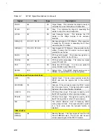
AEN
173
O
ISA I/O Address Enable. Active high signal during DMA
cycle to prevent I/O device from misinterpreting the DMA
cycle as valid I/O cycle.
IOCHRDY
172
I/O
ISA System Ready. This signal is an output during
ISA/DMA master cycle.
NOWSJ
169
I
ISA Zero-wait State for Input. This signal terminates the
CPU to ISA command instantly.
IOCHKJ
160
I
ISA Parity Error. M1523 generates NMI to CPU when this
signal is asserted.
SYSCLK
183
O
ISA System Clock. This signal provides clocking function
to ISA bus.
BALE
2
O
Bus Address Latch Enable. BALE is active throughout
DMA and ISA master and refresh cycles.
IORJ
180
I/O
ISA I/O Read. This signal is an input during ISA master
cycle.
IOWJ
178
I/O
ISA I/O Write. This signal is an input during ISA master
cycle.
Summary of Contents for AcerNote Light 370P
Page 6: ...vi ...
Page 26: ...1 8 Service Guide Figure 1 5 Main Board Layout Bottom Side ...
Page 49: ...System Introduction 1 31 1 5 1 3 Power Management Figure 1 14 Power Management Block Diagram ...
Page 55: ...System Introduction 1 37 1 6 System Block Diagram Figure 1 15 System Block Diagram ...
Page 64: ...Major Chips Description 2 7 2 2 5 Pin Diagram Figure 2 4 M1521 Pin Diagram ...
Page 99: ...2 42 Service Guide 2 5 3 Pin Diagram Figure 2 10 C T 65550 Pin Diagram ...
Page 117: ...2 60 Service Guide Figure 2 12 Functional block diagram CardBus Card Interface ...
Page 119: ...2 62 Service Guide Figure 2 14 PCI to CardBus terminal assignments ...
Page 135: ...2 78 Service Guide 2 7 3 Pin Diagram Figure 2 16 NS87336VJG Pin Diagram ...
Page 145: ...2 88 Service Guide 2 8 2 Pin Diagram Figure 2 17 YMF715 Block Diagram ...
Page 185: ...Disassembly and Unit Replacement 4 5 Figure 4 3 Disassembly Sequence Flowchart ...
Page 209: ...B 2 Service Guide ...
Page 210: ...Exploded View Diagram B 3 ...

