2-22
Service Guide
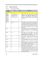
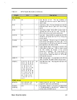
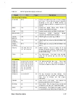
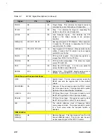
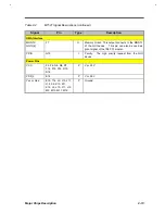
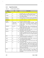
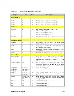
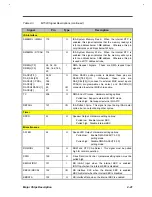
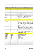
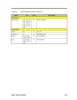
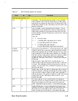
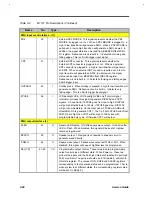
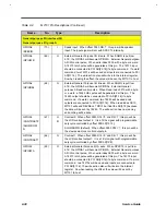
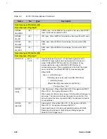
Table 2-3
M1523 Signal Descriptions (continued)
Signal
Pin
Type
Description
Miscellaneous
MSCLK
154
O
Mouse Clock Output when the internal KBC is enabled.
RTC32KI
16
I
RTC 32.768K Osc1. This is crystal input and requires an
external 32.768khz quartz crystal.
RTC32KII
15
I
RTC 32.768K Osc2. This is crystal input and requires an
external 32.768khz quartz crystal.
SIRQI
44
I
Steerable IRQ Input 1
SIRQII/IRQ8J
45
I
Steerable IRQ Input 2 when the internal RTC is enabled.
RTC interrupt input when the internal RTC is disabled.
USBCLK
46
I
Universal serial bus clock pin (reserved).
USBP1[1:0]
59, 60
I/O
Universal serial bus data pin (reserved).
Power Management
EXTSW /
APICREQJ
61
I
External SMI Switch or APIC Request Input. EXTSW is a
falling edge triggered input to the M1523 showing that an
external device is requesting the system to enter SMM
mode. An external pull-up should be placed on this signal
if it is not used or it is not guaranteed to be always driven.
When external APIC mode is enabled, this pin is
APICREQJ.
SMIJ / APICCSJ
50
O
SMM Interrupt or APIC Chip Select. A synchronous
output asserted by the M1523 in response to one of many
enabled hardware or software events. When external APIC
mode is enabled, this pin is APICCSJ.
STPCLKJ /
APICGNTJ
51
O
Stop CPU Clock Request or APIC Grant Output.
STPCLKJ is connected directly to the CPU and is
synchronous with PCI clock. When external APIC mode is
enabled, this pin is APICGNTJ.
IDE Interface
IDRQ[1:0]
138-137
I
IDE DRQ Request for IDE Master
IDAKJ[1:0]
143-142
O
IDE DACKJ for IDE Master
IDERDY
141
I
IDE Ready
IDEIORJ
140
O
IDE IORJ Command
IDEIOWJ
139
O
IDE IOWJ Command
IDESCS1J
149
O
IDE chip Select for Secondary Channel 0
IDESCS3J
150
O
IDE chip Select for Secondary Channel 1
IDEPCS1J
147
O
IDE chip Select for Primary Channel 0
IDEPCS3J
148
O
IDE chip Select for Primary Channel 1
IDE_A[2:0]
145, 144, 146
O
IDE ATA Address Bus
Summary of Contents for AcerNote Light 370P
Page 6: ...vi ...
Page 26: ...1 8 Service Guide Figure 1 5 Main Board Layout Bottom Side ...
Page 49: ...System Introduction 1 31 1 5 1 3 Power Management Figure 1 14 Power Management Block Diagram ...
Page 55: ...System Introduction 1 37 1 6 System Block Diagram Figure 1 15 System Block Diagram ...
Page 64: ...Major Chips Description 2 7 2 2 5 Pin Diagram Figure 2 4 M1521 Pin Diagram ...
Page 99: ...2 42 Service Guide 2 5 3 Pin Diagram Figure 2 10 C T 65550 Pin Diagram ...
Page 117: ...2 60 Service Guide Figure 2 12 Functional block diagram CardBus Card Interface ...
Page 119: ...2 62 Service Guide Figure 2 14 PCI to CardBus terminal assignments ...
Page 135: ...2 78 Service Guide 2 7 3 Pin Diagram Figure 2 16 NS87336VJG Pin Diagram ...
Page 145: ...2 88 Service Guide 2 8 2 Pin Diagram Figure 2 17 YMF715 Block Diagram ...
Page 185: ...Disassembly and Unit Replacement 4 5 Figure 4 3 Disassembly Sequence Flowchart ...
Page 209: ...B 2 Service Guide ...
Page 210: ...Exploded View Diagram B 3 ...

