Major Chips Description
2-23
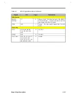
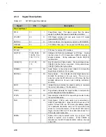
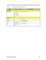
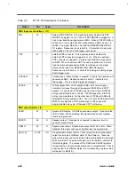
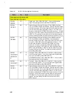
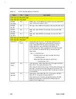
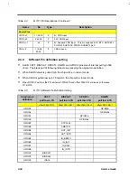
Table 2-3
M1523 Signal Descriptions (continued)
Signal
Pin
Type
Description
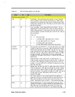
IDE Interface
IDE_D[15:0]
135, 132, 130,
128, 126, 124,
122, 119, 121,
123, 125, 127,
129, 131, 133,
136
I/O
IDE ATA Data Bus
Vcc and Vss
VCC3
53
P
Vcc 3.3V
VCC5/V
BAT
14
P
RTC Battery Input
VCC5
40, 72, 105,
120, 156, 208
P
VCC 5.0V(VDD)
Vss
1, 26, 52, 82,
104, 134, 157,
182
P
Vss or Ground.
Summary of Contents for AcerNote Light 370P
Page 6: ...vi ...
Page 26: ...1 8 Service Guide Figure 1 5 Main Board Layout Bottom Side ...
Page 49: ...System Introduction 1 31 1 5 1 3 Power Management Figure 1 14 Power Management Block Diagram ...
Page 55: ...System Introduction 1 37 1 6 System Block Diagram Figure 1 15 System Block Diagram ...
Page 64: ...Major Chips Description 2 7 2 2 5 Pin Diagram Figure 2 4 M1521 Pin Diagram ...
Page 99: ...2 42 Service Guide 2 5 3 Pin Diagram Figure 2 10 C T 65550 Pin Diagram ...
Page 117: ...2 60 Service Guide Figure 2 12 Functional block diagram CardBus Card Interface ...
Page 119: ...2 62 Service Guide Figure 2 14 PCI to CardBus terminal assignments ...
Page 135: ...2 78 Service Guide 2 7 3 Pin Diagram Figure 2 16 NS87336VJG Pin Diagram ...
Page 145: ...2 88 Service Guide 2 8 2 Pin Diagram Figure 2 17 YMF715 Block Diagram ...
Page 185: ...Disassembly and Unit Replacement 4 5 Figure 4 3 Disassembly Sequence Flowchart ...
Page 209: ...B 2 Service Guide ...
Page 210: ...Exploded View Diagram B 3 ...

