2-30
Service Guide
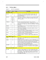
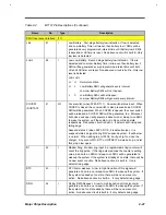
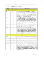
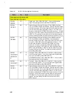
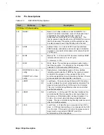
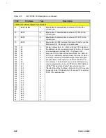
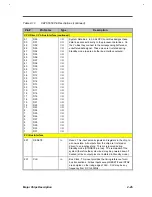
Table 2-4
M7101 Pin Descriptions (Continued)
Name
No.
Type
Description
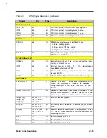
General purpose I/O interface(24)
General purpose I/O group A
GPIOA6
/SPEKIN
(70)
I
Speak input. When offset 0F6h D6=‘1’, this pin will be speaker
input. The input signal will xor with SPKCTL internally.
GPIOA5
/GPIOWB
(69)
O
External General Purpose I/O B write. When SQWO is pull low
4.7K, the GPIOA5 will become GPIOWA. External General purpose
A R/W control pulse, When write index 0F0h with a byte or a word.
A 74373 latch pulse will be generated at this pin. The 74373 input
should be connected to PCI AD[23:16] if a byte command. If a word
command, two 74373s will be used and inputs are connected to PCI
AD[31:16]. The write action also will write into the internal register.
So when reading the offset, the value will be sent by M7101 to host.
GPIOA4
/GPIORBJ
(68)
O
External General Purpose I/O B read. When SQWO is pull low
4.7K, the GPIOA0 will become GPIORAJ. External General
purpose A Read control pulse. When Read index 0F1h with a byte
or a word, a 74245 OEJ pulse will be generated at this pin. The
74245 output should be connected to PCI AD[23:16] if a byte
command. If a word command, two 74245 will be used and4
outputs are connected to PCI AD[31:16]. When read index 0E1h,
M7101 will send DEVSELJ, TRDYJ but float the AD[31:0] because
the data will be sent by 74245. The write action has no meaning
and nothing will be done.
GPIOA3
/CONTRAST2
/SLOWDOW
N
(67)
O
/O
Contrast2. When offset 0F6h D14=‘0’ and D9=‘1’, this pin will be
the LCD contrast output 2. It is a 1Khz signal with programmable
duty cycle controlled by offset 0FBh D[15:13].
SLOWDOWN (default). When offset 0F6h D14=‘1’, this pin will be
the slow down clock control output pin.
GPIOA2
/CONTRAST1
(66)
O
Contrast1. When offset 0F6h D14=’0’ and D8=’1’, this pin will be
the LCD contrast output1. It is a 1 KHz signal with programmable
duty cycle controlled by offset 0FBh D[12:8].
GPIOA1
/GPIOWA
(65)
O
External General Purpose I/O A write. When SPKCTL is pull low
4.7K, the GPIOA1 will become GPIOWA. External General purpose
A R/W control pulse, When write index 0E0h with a byte or a word.
A 74373 latch pulse will be generated at this pin, The 74373 input
should be connected to PCI AD[23:16] if a byte command. If a word
command , two 74373s will be used and inputs are connected to
PCI AD[31:16]. The write action also will write into the internal
register. So when reading the offset, the value will be sent by
M7101 to host.
Summary of Contents for AcerNote Light 370P
Page 6: ...vi ...
Page 26: ...1 8 Service Guide Figure 1 5 Main Board Layout Bottom Side ...
Page 49: ...System Introduction 1 31 1 5 1 3 Power Management Figure 1 14 Power Management Block Diagram ...
Page 55: ...System Introduction 1 37 1 6 System Block Diagram Figure 1 15 System Block Diagram ...
Page 64: ...Major Chips Description 2 7 2 2 5 Pin Diagram Figure 2 4 M1521 Pin Diagram ...
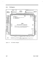
Page 99: ...2 42 Service Guide 2 5 3 Pin Diagram Figure 2 10 C T 65550 Pin Diagram ...
Page 117: ...2 60 Service Guide Figure 2 12 Functional block diagram CardBus Card Interface ...
Page 119: ...2 62 Service Guide Figure 2 14 PCI to CardBus terminal assignments ...
Page 135: ...2 78 Service Guide 2 7 3 Pin Diagram Figure 2 16 NS87336VJG Pin Diagram ...
Page 145: ...2 88 Service Guide 2 8 2 Pin Diagram Figure 2 17 YMF715 Block Diagram ...
Page 185: ...Disassembly and Unit Replacement 4 5 Figure 4 3 Disassembly Sequence Flowchart ...
Page 209: ...B 2 Service Guide ...
Page 210: ...Exploded View Diagram B 3 ...

