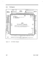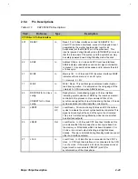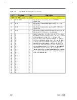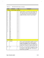
2-38
Service Guide
2.4.7
Function Description
The function blocks of M7101 are as follows :
1. PCI Interface
2. State Controller
3. Timer
4. Wake up event handler
5. Activity monitor
6. Battery monitor
7. General Purpose Input/Output (GPIO)
8. SMIJ Generator
9. SUSPEND monitor
10. APM monitor
11. Rundown Emulation
12. LCD control
13. SLOWDOWN control
PCI interface
The PCI interface is running at PCICLK frequency. From the point of PCI bus, M7101 is a hidden
component. There are no PCI configuration spaces built in. So using PCI configuration read/write
method cannot detect the existence of M7101.
M7101 just decodes the I/O 0178h/017Ah or 0078h/007Ah address. When it detects the address,
it will assert the DEVSELJ signal and TRDYJ when data is ready. M7101 is only a PCI slave
device, no REQJ and GNTJ signal required. All the PCI interface timing can meet the
requirements of PCI spec. V2.1.
M7101 will monitor the PCI bus behavior to detect the Device access like HDD, SIO, PIO, VGA
memory range, Floppy, KBC and IO&MEM group. It will decode these addresses but not assert
DEVSELJ. The interface is static design. So the input PCICLK can be changed from 33 MHz to 0
Hz without glitch.
There is a Lock register at offset 0D1h. When set D5 to 1 will unlock I/O port 017Ah/007Ah. Host
can read or write I/O port 017Ah/007Ah. When set D5 to 0, then Host cannot I/O read/write I/O
port 017Ah/007Ah except the offset 0D1h. No matter lock or unlock, when access to I/O port
017Ah, DEVSELJ will always be active.
Summary of Contents for AcerNote Light 370P
Page 6: ...vi ...
Page 26: ...1 8 Service Guide Figure 1 5 Main Board Layout Bottom Side ...
Page 49: ...System Introduction 1 31 1 5 1 3 Power Management Figure 1 14 Power Management Block Diagram ...
Page 55: ...System Introduction 1 37 1 6 System Block Diagram Figure 1 15 System Block Diagram ...
Page 64: ...Major Chips Description 2 7 2 2 5 Pin Diagram Figure 2 4 M1521 Pin Diagram ...
Page 99: ...2 42 Service Guide 2 5 3 Pin Diagram Figure 2 10 C T 65550 Pin Diagram ...
Page 117: ...2 60 Service Guide Figure 2 12 Functional block diagram CardBus Card Interface ...
Page 119: ...2 62 Service Guide Figure 2 14 PCI to CardBus terminal assignments ...
Page 135: ...2 78 Service Guide 2 7 3 Pin Diagram Figure 2 16 NS87336VJG Pin Diagram ...
Page 145: ...2 88 Service Guide 2 8 2 Pin Diagram Figure 2 17 YMF715 Block Diagram ...
Page 185: ...Disassembly and Unit Replacement 4 5 Figure 4 3 Disassembly Sequence Flowchart ...
Page 209: ...B 2 Service Guide ...
Page 210: ...Exploded View Diagram B 3 ...

