A p
A p p e n d
p e n d i x E
i x E
BIOS POST Checkpoints
BIOS POST Checkpoints
E-1
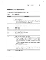
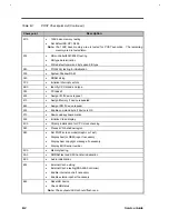
This appendix lists the POST checkpoints of the notebook BIOS.
Table E-1
POST Checkpoint List
Checkpoint
Description
04h
•
Check CPU ID
•
Dispatch Shutdown Path
Note: At the beginning of POST, port 64 bit 2 (8042 system flag) is read to
determine whether this POST is caused by a cold or warm boot. If it is a cold
boot, a complete POST is performed. If it is a warm boot, the chip initialization
and memory test is eliminated from the POST routine.
08h
•
Reset PIE, AIE, UIE
Note: These interrupts are disabled in order to avoid any incorrect actions from
happening during the POST routine.
09h
•
Initialize m1511
0Ah
•
Initialize m1513
0Bh
•
Initialize m7101
10h
•
DMA(8237) testing & initialization
14h
•
System Timer(8254) testing & initialization
18h
•
DRAM refresh cycle testing
•
Set default SS:SP= 0:400
1Ch
•
CMOS shutdown byte test, battery, and check sum
Note: Several parts of the POST routine require the system to be in protected
mode. When returning to real mode from protected mode, the processor is
reset, therefore POST is re-entered. In order to prevent re-initialization of the
system, POST reads the shutdown code stored in location 0Fh in CMOS
RAM. Then it jumps around the initialization procedure to the appropriate
entry point.
The CMOS shutdown byte verification assures that CMOS 0Fh area is fine to
execute POST properly.
•
Initialize default CMOS setting if CMOS bad
•
Initialize RTC time base
Note: The RTC has an embedded oscillator that generates 32.768 KHz frequency.
To initialize the RTC time base, turn on this oscillator and set a divisor to
32768 so that the RTC can count time correctly
1Dh, 1Eh
•
DRAM type determination
Summary of Contents for AcerNote Light 370P
Page 6: ...vi ...
Page 26: ...1 8 Service Guide Figure 1 5 Main Board Layout Bottom Side ...
Page 49: ...System Introduction 1 31 1 5 1 3 Power Management Figure 1 14 Power Management Block Diagram ...
Page 55: ...System Introduction 1 37 1 6 System Block Diagram Figure 1 15 System Block Diagram ...
Page 64: ...Major Chips Description 2 7 2 2 5 Pin Diagram Figure 2 4 M1521 Pin Diagram ...
Page 99: ...2 42 Service Guide 2 5 3 Pin Diagram Figure 2 10 C T 65550 Pin Diagram ...
Page 117: ...2 60 Service Guide Figure 2 12 Functional block diagram CardBus Card Interface ...
Page 119: ...2 62 Service Guide Figure 2 14 PCI to CardBus terminal assignments ...
Page 135: ...2 78 Service Guide 2 7 3 Pin Diagram Figure 2 16 NS87336VJG Pin Diagram ...
Page 145: ...2 88 Service Guide 2 8 2 Pin Diagram Figure 2 17 YMF715 Block Diagram ...
Page 185: ...Disassembly and Unit Replacement 4 5 Figure 4 3 Disassembly Sequence Flowchart ...
Page 209: ...B 2 Service Guide ...
Page 210: ...Exploded View Diagram B 3 ...

