1-
14
Service Guide
1.4
Hardware Configuration and Specification
1.4.1
Memory Address Map
Table 1-7
Memory Address Map
Address Range
Definition
Function
000000 - 09FFFF
640 KB memory
Base memory
0A0000 - 0BFFFF
128 KB video RAM
Reserved for graphics display buffer
0C0000 - 0CBFFF
Video BIOS
Video BIOS
0E0000 - 0EFFFF
0F0000 - 0FFFFF
128 KB system BIOS
System BIOS
System BIOS
10000 - 7FFFF
80000 - 27FFF
Extended memory
Onboard Memory
SIMM memory
FE0000 - FFFFFF
256 KB system ROM
Duplicate of code assignment at 0E0000-0FFFFF
1.4.2
Interrupt Channel Map
Table 1-8
Interrupt Channel Map
Priority
Interrupt Number
Interrupt Source
1
2
3
4
5
6
7
8
9
10
11
12
13
14
15
16
17
SMI
NMI
IRQ 0
IRQ 1
IRQ 2
IRQ 8
IRQ 9
IRQ 10
IRQ 11
IRQ 12
IRQ 13
IRQ 14
IRQ 15
IRQ 3
IRQ 4
IRQ 5
IRQ 6
IRQ 7
Power management unit
Parity error detected, I/O channel error
Interval timer, counter 0 output
Keyboard
Interrupt from controller 2 (cascade)
Real-time clock
Cascaded to INT 0AH (IRQ 2)
Audio (option) / PCMCIA
Audio (option) / PCMCIA
PS/2 mouse
INT from coprocessor
Hard disk controller
CD-ROM controller
Serial communication port 2
Serial communication port 1
Parallel port (option) / Audio
Diskette controller
Parallel port (option)
A PCMCIA card can use IRQ 3, 4, 5, 7, 9 and 11 as long as it does not conflict with the
interrupt address of any other device.
1.4.3
DMA Channel Map
Table 1-9
DMA Channel Map
Controller
Channel
Address
Function
1
0
0087
Audio (option)/ECP(option)
Summary of Contents for AcerNote Light 370P
Page 6: ...vi ...
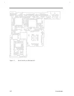
Page 26: ...1 8 Service Guide Figure 1 5 Main Board Layout Bottom Side ...
Page 49: ...System Introduction 1 31 1 5 1 3 Power Management Figure 1 14 Power Management Block Diagram ...
Page 55: ...System Introduction 1 37 1 6 System Block Diagram Figure 1 15 System Block Diagram ...
Page 64: ...Major Chips Description 2 7 2 2 5 Pin Diagram Figure 2 4 M1521 Pin Diagram ...
Page 99: ...2 42 Service Guide 2 5 3 Pin Diagram Figure 2 10 C T 65550 Pin Diagram ...
Page 117: ...2 60 Service Guide Figure 2 12 Functional block diagram CardBus Card Interface ...
Page 119: ...2 62 Service Guide Figure 2 14 PCI to CardBus terminal assignments ...
Page 135: ...2 78 Service Guide 2 7 3 Pin Diagram Figure 2 16 NS87336VJG Pin Diagram ...
Page 145: ...2 88 Service Guide 2 8 2 Pin Diagram Figure 2 17 YMF715 Block Diagram ...
Page 185: ...Disassembly and Unit Replacement 4 5 Figure 4 3 Disassembly Sequence Flowchart ...
Page 209: ...B 2 Service Guide ...
Page 210: ...Exploded View Diagram B 3 ...

