1-
16
Service Guide
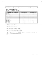
1.4.5
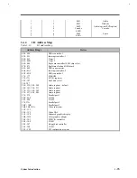
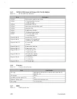
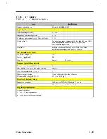
M7101 GPIO (General Purpose I/O) Port Definition
Table 1-11
M7101 GPIO Port Definition
Item
Description
GPIOA2
Smart inverter contrast counter control
GPIOA3
0: Normal operation of system
1: Shutdown system
GPIOA4
Serial data on X24C02
GPIOA5
Battery gauge communication control
GPIOA6
Battery data line
GPIOA7
Thermal sensor data line
GPIOC6
VGA thermal sensor data line
GPIOC7
0: VGA chip standby mode
1: Normal operation
Register E0h bit 8
Serial clock on X24C02
Register E0h bit 9
0: Disable 12V for flash ROM
1: Enable 12V for flash ROM
Register E0h bit 10
0: 3 mode FDD
1: Normal
Register E0h bit 11
Thermal sensor clock line
Register E0h bit 12
Thermal sensor reset
Register E0h bit 13
0: Enable battery LED
1: Disable battery LED
Register E0h bit 14
0: Disable audio amplifier
1: Enable audio amplifier
Register E1h bit 0
0: NiMH battery
1: Li-ion battery
Register E1h bit 1
CPU thermal high
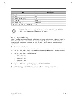
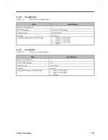
1.4.6
Processor
Table 1-12
Processor Specifications
Item
Specification
CPU type
P54CSLM-120,P54CSLM-133, P54CSLM-150, P55CLM-133,
P55CLM - 150
CPU package
SPGA
Switchable processor speed (Y/N)
Yes
Minimum working speed
0MHz while hibernation mode
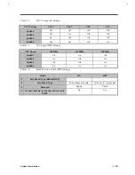
CPU voltage
3.1V/2.9V/2.45V
1.4.7
BIOS
Table 1-13
BIOS Specifications
Summary of Contents for AcerNote Light 370P
Page 6: ...vi ...
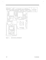
Page 26: ...1 8 Service Guide Figure 1 5 Main Board Layout Bottom Side ...
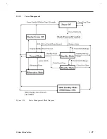
Page 49: ...System Introduction 1 31 1 5 1 3 Power Management Figure 1 14 Power Management Block Diagram ...
Page 55: ...System Introduction 1 37 1 6 System Block Diagram Figure 1 15 System Block Diagram ...
Page 64: ...Major Chips Description 2 7 2 2 5 Pin Diagram Figure 2 4 M1521 Pin Diagram ...
Page 99: ...2 42 Service Guide 2 5 3 Pin Diagram Figure 2 10 C T 65550 Pin Diagram ...
Page 117: ...2 60 Service Guide Figure 2 12 Functional block diagram CardBus Card Interface ...
Page 119: ...2 62 Service Guide Figure 2 14 PCI to CardBus terminal assignments ...
Page 135: ...2 78 Service Guide 2 7 3 Pin Diagram Figure 2 16 NS87336VJG Pin Diagram ...
Page 145: ...2 88 Service Guide 2 8 2 Pin Diagram Figure 2 17 YMF715 Block Diagram ...
Page 185: ...Disassembly and Unit Replacement 4 5 Figure 4 3 Disassembly Sequence Flowchart ...
Page 209: ...B 2 Service Guide ...
Page 210: ...Exploded View Diagram B 3 ...

