2-18
Service Guide
2.3.4
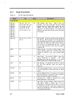
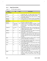
Signal Descriptions
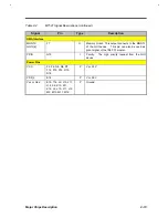
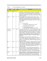
Table 2-3
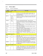
M1523 Signal Descriptions
Signal
Pin
Type
Description
Clock and Reset
PWG
17
I
Power-Good Input. This signal comes from the power
supply to indicate that power is available and stable.
CPURST
49
O
CPU Reset includes cold and warm reset 3.3V signal
(connected to CPU INIT)
RSTDRV
57
O
CPU Cold Reset. 3.3V signal (connected to CPU RESET)
OSC14M
43
I
14.318Mhz Clock Input. This is used for 8254 timer clock.
PCI Interface
PCICLK
71
I
PCI clock for internal PCI interface.
AD[31:0]
73-80, 83-90,
100-104, 106-
109, 111-118
I/O
Address and Data are multiplexed on PCI bus. During
the first clock of a PCI transaction, AD[31-0] contains a
physical address. During subsequent clocks, AD[31-0]
contains data.
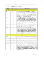
C/BEJ[3:0]
81, 91, 99,
110
I/O
Bus Command and Byte Enable. During address phase,
CBEJ[3:0] define the bus command. During data phase,
CBEJ[3:0] define the byte enables.
FRAMEJ
92
I/O
Cycle Frame. is driven by current initiator to indicate the
beginning and duration of an access.
DEVSELJ
95
I/O
Device Select. . This indicates that the target device has
decoded the address as its own cycle. This pin is an
output pin when the M1523 acts as a PCI slave that has
decoded address as its own cycle including subtractive
decoding.
IRDYJ
93
I/O
Initiator Ready indicates the initiator’s ability to complete
the current data phase of the transaction.
TRDYJ
94
I/O
Target Ready indicates the target's ability to complete the
current data phase of the transaction.
STOPJ
96
I/O
Stop indicates to the M1523 is requesting a master to stop
the current transaction.
PAR
98
I/O
Parity Signal. PAR is even parity and is calculated on
AD[31:0] and CBEJ[3:0]. When the M1523 acts as a PCI
master, it drives PAR one PCI clock after address phase
for a read/write transaction and one PCI clock after data
phase for a write transaction. When the M1523 acts as
target, it drives PAR one PCI clock after data phase for a
PCI master read transaction.
SERRJ
97
I
System Error may be pulsed active by any agent that
detects a system error condition. When SERRJ is
sampled low, the M1523 asserts NMI to send an interrupt
to the CPU.
Summary of Contents for AcerNote Light 370P
Page 6: ...vi ...
Page 26: ...1 8 Service Guide Figure 1 5 Main Board Layout Bottom Side ...
Page 49: ...System Introduction 1 31 1 5 1 3 Power Management Figure 1 14 Power Management Block Diagram ...
Page 55: ...System Introduction 1 37 1 6 System Block Diagram Figure 1 15 System Block Diagram ...
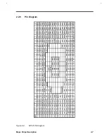
Page 64: ...Major Chips Description 2 7 2 2 5 Pin Diagram Figure 2 4 M1521 Pin Diagram ...
Page 99: ...2 42 Service Guide 2 5 3 Pin Diagram Figure 2 10 C T 65550 Pin Diagram ...
Page 117: ...2 60 Service Guide Figure 2 12 Functional block diagram CardBus Card Interface ...
Page 119: ...2 62 Service Guide Figure 2 14 PCI to CardBus terminal assignments ...
Page 135: ...2 78 Service Guide 2 7 3 Pin Diagram Figure 2 16 NS87336VJG Pin Diagram ...
Page 145: ...2 88 Service Guide 2 8 2 Pin Diagram Figure 2 17 YMF715 Block Diagram ...
Page 185: ...Disassembly and Unit Replacement 4 5 Figure 4 3 Disassembly Sequence Flowchart ...
Page 209: ...B 2 Service Guide ...
Page 210: ...Exploded View Diagram B 3 ...

