11
F-2
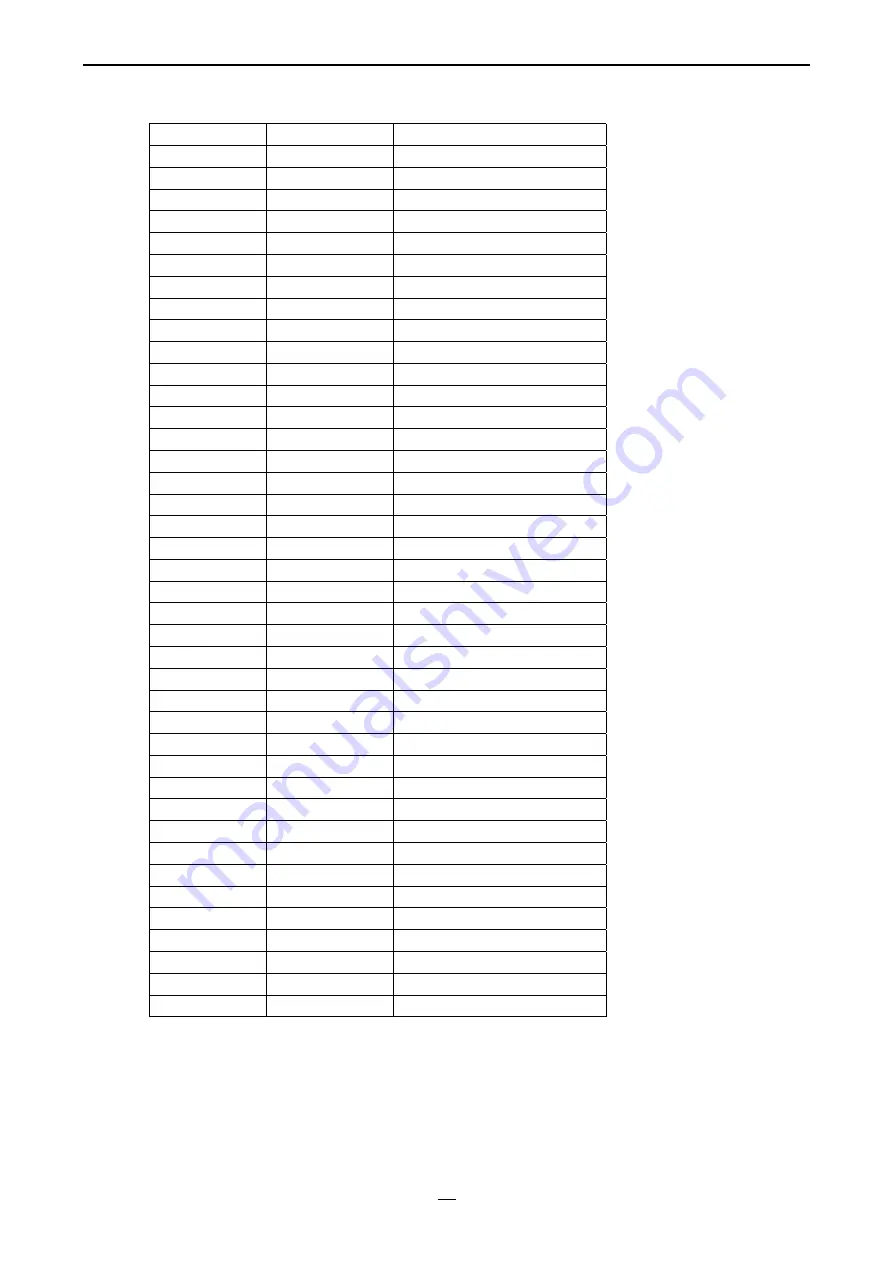
CN3
Terminal No.
Symbol
Function
1
VDD1
Digital Power Input (DC+3.3V)
2
VDD1
Digital Power Input (DC+3.3V)
3 GND
Ground
4 GND
Ground
5
0B5
Odd-dot Blue Data bit 5 (MSB)
6
0B4
Odd-dot Blue Data bit 4
7
0B3
Odd-dot Blue Data bit 3
8
0B2
Odd-dot Blue Data bit 2
9
0B1
Odd-dot Blue Data bit 1
10
0B0
Odd-dot Blue Data bit 0
11 GND
Ground
12
0G5
Odd-dot Green Data bit 5 (MSB)
13
0G4
Odd-dot Green Data bit 4
14
0G3
Odd-dot Green Data bit 3
15
0G2
Odd-dot Green Data bit 2
16
0G1
Odd-dot Green Data bit 1
17
0G0
Odd-dot Green Data bit 0 (LSB)
18 GND
Ground
19
0R5
Odd-dot Red Data bit 5 (MSB)
20
0R4
Odd-dot Red Data bit 4
21
0R3
Odd-dot Red Data bit 3
22
0R2
Odd-dot Red Data bit 2
23
0R1
Odd-dot Red Data bit 1
24
0R0
Odd-dot Red Data bit 0 (LSB)
25 GND
Ground
26
CPH2
Pixel Clock Input
27 GND
Ground
28 GND
Ground
29 NC
No
connecting
30 NC
No
connecting
31
VGH
Gate Driver High Voltage Input
32 NC
No
connecting
33
VGL
Gate Driver Low Voltage Input
34 NC
No
connecting
35
VGC
Gate Driver Common Voltage Input
36 NC
No
connecting
37 NC
No
connecting
38 NC
No
connecting
39 GND
Ground
40 GND
Ground
Summary of Contents for AL501
Page 23: ...23 10 TROUBLESHOOTING A Main Procedure ...
Page 24: ...24 A 1 Power Circuit Troubleshooting ...
Page 25: ...25 A 2 Backlights Troubleshooting ...
Page 26: ...26 A 3 Performance Troubleshooting ...
Page 27: ...27 A 4 Function Troubleshooting ...
Page 28: ...28 APPENDIX A PARTS LISTS ...
Page 29: ...29 A FRU BOM A 1 453A5730021 PCBA Inverter board A 2 454A6930011 PCBA Key Board ...


