146
Chapter 5
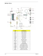
Bottom View
ITEM
DESCRIPTION
PJP1
AC-IN Connector
JRJ45
RJ45 Connector
JCRT1
CRT Connector
JP12
Fan Connector
JUSB1
USB Connector
JUSB2
USB Connector
JMIC1
MIC-In Jack
JHP1
Head-Phone Jack
JSATA2
HDD Connector
U23
North Bridge
JCPU1
CPU Socket
JREAD1
Card Reader Socket
PJP3
Battery Board Connector
JDIMM2
Memory DIMM2 Connector
JDIMM1
Memory DIMM1 Connector
PJP2
ODD Board Connector
JMINI2
Wireless Card Connector
Summary of Contents for AS7315-302G25Mn
Page 6: ...VI ...
Page 10: ...X Table of Contents ...
Page 13: ...Chapter 1 3 System Block Diagram ...
Page 30: ...20 Chapter 1 ...
Page 52: ...42 Chapter 2 ...
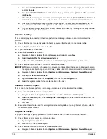
Page 74: ...64 Chapter 3 4 Disconnect the following four cables from the Mainboard A B C D ...
Page 87: ...Chapter 3 77 4 Using both hands lift the Thermal Module clear of the Mainboard ...
Page 89: ...Chapter 3 79 4 Lift the CPU Fan clear of the Mainboard as shown ...
Page 95: ...Chapter 3 85 5 Lift the LCD Panel clear of the module ...
Page 103: ...Chapter 3 93 9 The Antennas and cables appear as shown when correctly installed ...
Page 108: ...98 Chapter 3 2 Replace the four screws and screw caps provided ...
Page 113: ...Chapter 3 103 5 Replace the FFC and press down as indicated to secure it to the Upper Cover ...
Page 124: ...114 Chapter 3 17 Replace the two screws securing the LCD Module to the Lower Cover ...
Page 132: ...122 Chapter 3 ...
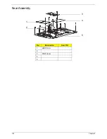
Page 164: ...154 Chapter 6 Rear Assembly No Description Acer P N 1 HDD Cover 2 3 RAM Cover 4 5 1 2 3 4 5 ...
Page 174: ...Appendix A 164 Model Definition and Configuration Appendix A ...
Page 196: ...186 Appendix C ...
Page 200: ...190 ...

