167
Chapter 4
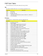
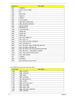
DLL Timing Control Registers, RCOMP settings
Post Code
Description
0x27
Enable DRAM Channel I/O Buffers
0x28
Enable all clocks on populated rows
0x29
Perform JEDEC memory initialization for all memory rows
0x30
Perform steps required after memory init
0x31
Program DRAM throttling and throttling event registers
0x32
Setup DRAM control register for normal operation and enable
0x33
Enable RCOMP
0x34
Clear DRAM initialization bit in the SB
0x35
Initialization Sequence Completed, program graphic clocks
0x43
Program Thermal Throttling
Summary of Contents for Aspire 5534 Series
Page 6: ...VI ...
Page 10: ...X Table of Contents ...
Page 32: ...22 Chapter 1 ...
Page 51: ...Chapter 2 41 ...
Page 52: ...42 Chapter 2 ...
Page 65: ...Chapter 3 55 ...
Page 79: ...Chapter 3 69 ...
Page 81: ...Chapter 3 71 5 Lift the Power Board from the Lower Cover ...
Page 83: ...Chapter 3 73 6 Lift the right side speaker out from the Lower Cover as shown ...
Page 89: ...Chapter 3 79 7 Disconnect the I O Board Cable from the I O Board ...
Page 97: ...Chapter 3 87 ...
Page 103: ...Chapter 3 93 ...
Page 107: ...Chapter 3 97 6 Disconnect the LCD cable as shown and remove the cable from the LCD Panel ...
Page 110: ...100 Chapter 3 ...
Page 197: ...Chapter 6 187 ...
Page 224: ...214 ...

