138
Chapter 4
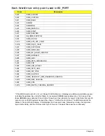
BDS & Specific action:
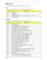
0x27
Enable DRAM Channel I/O Buffers
0x28
Enable all clocks on populated rows
0x29
Perform JEDEC memory initialization for all memory rows
0x30
Perform steps required after memory init
0x31
Program DRAM throttling and throttling event registers
0x32
Setup DRAM control register for normal operation and enable
0x33
Enable RCOMP
0x34
Clear DRAM initialization bit in the SB
0x35
Initialization Sequence Completed, program graphic clocks
0xAF
Disable access to the XMM registers
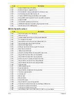
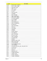
Code
Description
0x00
Report the legacy boot is happening
0x12
Wake up the Aps
0x13
Initialize SMM Private Data and relocate BSP SMBASE
0x21
PC init begin at the stage1
0x27
Report every memory range do the hardware ECC init
0x28
Report status code of every memory range
0x50
Get the root bridge handle
0x51
Notify pci bus driver starts to program the resource
0x58
Reset the host controller
0x5A
IdeBus begin initialization
0x70
Simple Text Output Protocol Functions(VGA class reset)
0x71
Report that VGA Class driver is being disabled
0x72
Report that VGA Class driver is being enabled
0x78
Terminal Console In reset and Console Out reset
0x79
Report that the remote terminal is being disabled
0x7A
Report that the remote terminal is being enabled
0x90
Keyboard reset
0x91
USB Keyboard disable
0x92
Keyboard detection
0x93
Report that the usb keyboard is being enabled
0x94
Clear the keyboard buffer
0x95
Init Keyboard
0x98
Mouse reset
0x99
Mouse disable
0x9A
Detect PS2 mouse
0x9B
Report that the mouse is being enabled
0xB8
Peripheral removable media reset (ex: IsaFloppy, USB device)
0xB9
Peripheral removable media disable
0xBB
Peripheral removable media enable
0xE4
Report Status Code here for DXE_ENTRY_POINT once it is available
Code
Description
Summary of Contents for Aspire 7715Z Series
Page 6: ...VI ...
Page 10: ...X Table of Contents ...
Page 13: ...Chapter 1 3 System Block Diagram ...
Page 30: ...20 Chapter 1 ...
Page 52: ...42 Chapter 2 ...
Page 74: ...64 Chapter 3 4 Disconnect the following four cables from the Mainboard A B C D ...
Page 87: ...Chapter 3 77 4 Using both hands lift the Thermal Module clear of the Mainboard ...
Page 89: ...Chapter 3 79 4 Lift the CPU Fan clear of the Mainboard as shown ...
Page 95: ...Chapter 3 85 5 Lift the LCD Panel clear of the module ...
Page 103: ...Chapter 3 93 9 The Antennas and cables appear as shown when correctly installed ...
Page 108: ...98 Chapter 3 2 Replace the four screws and screw caps provided ...
Page 113: ...Chapter 3 103 5 Replace the FFC and press down as indicated to secure it to the Upper Cover ...
Page 124: ...114 Chapter 3 17 Replace the two screws securing the LCD Module to the Lower Cover ...
Page 132: ...122 Chapter 3 ...
Page 164: ...154 Chapter 6 Rear Assembly No Description Acer P N 1 HDD Cover 2 3 RAM Cover 4 5 1 2 3 4 5 ...
Page 174: ...Appendix A 164 Model Definition and Configuration Appendix A ...
Page 196: ...186 Appendix C ...
Page 200: ...190 ...

