Chapter 4
151
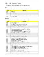
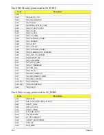
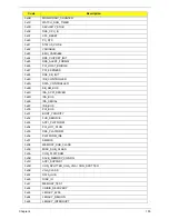
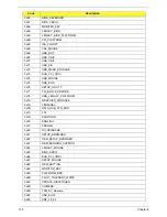
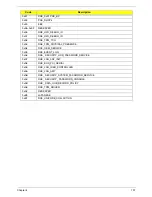
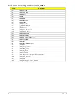
POST Code Reference Tables
These tables describe the POST codes and components of the POST process.
Sec:
NO_EVICTION_MODE_DEBUG EQU 1 (CommonPlatform\sec\Ia32\SecCore.inc)
Memory:
DEBUG_BIOS equ 1 (Chipset\Alviso\MemoryInitAsm\IA32\IMEMORY.INC)
Code
Description
0xC2
MTRR setup
0xC3
Enable cache
0xC4
Establish cache tags
0xC5
Enter NEM, Place the BSP in No Fill mode, set CR0.CD = 1, CR0.NW = 0.
0xCF
Cache Init Finished
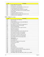
Code
Description
0xA0
First memory check point
0x01
Enable MCHBAR
0x02
Check for DRAM initialization interrupt and reset fail
0x03
Verify all DIMMs are DDR or DDR2 and unbuffered
0x04
Detect an improper warm reset and handle
0x05
Detect if ECC SO-DIMMs are present in the system
0x06
Verify all DIMMs are single or double sided and not asymmetric
0x07
Verify all DIMMs are x8 or x16 width
0x08
Find a common CAS latency between the DIMMS and the MCH
0x09
Determine the memory frequency and CAS latency to program
0x10
Determine the smallest common TRAS for all DIMMs
0x11
Determine the smallest common TRP for all DIMMs
0x12
Determine the smallest common TRCD for all DIMMs
0x13
Determine the smallest refresh period for all DIMMs
0x14
Verify burst length of 8 is supported by all DIMMs
0x15
Determine the smallest tWR supported by all DIMMs
0x16
Determine DIMM size parameters
0x17
Program the correct system memory frequency
0x18
Determine and set the mode of operation for the memory channels
0x19
Program clock crossing registers
0x20
Disable Fast Dispatch
0x21
Program the DRAM Row Attributes and DRAM Row Boundary registers
0x22
Program the DRAM Bank Architecture register
0x23
Program the DRAM Timing & and DRAM Control registers
0x24
Program ODT
0x25
Perform steps required before memory init
0x26
Program the receive enable reference timing control register
Program the DLL Timing Control Registers, RCOMP settings
Summary of Contents for Aspire One AO531h
Page 6: ...VI ...
Page 10: ...X Table of Contents ...
Page 30: ...20 Chapter 1 ...
Page 48: ...38 Chapter 2 ...
Page 63: ...Chapter 3 53 8 Disconnect the FFC and remove the Keyboard ...
Page 69: ...Chapter 3 59 4 Remove the board from the Upper Cover ...
Page 82: ...72 Chapter 3 5 Disconnect the Bluetooth cable from the module ...
Page 89: ...Chapter 3 79 4 Lift the CPU Fan clear of the Mainboard ...
Page 101: ...Chapter 3 91 4 Lift up the bezel and remove it from the LCD Module ...
Page 107: ...Chapter 3 97 7 Disconnect the cable from the LCD panel as shown ...
Page 138: ...128 Chapter 3 6 Insert the FFC in to the Button Board and close the locking latch ...
Page 202: ...192 Appendix B ...
Page 204: ...194 Appendix C ...
Page 208: ...198 ...

