Major Chips Description
2-53
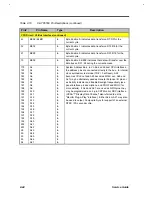
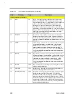
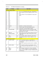
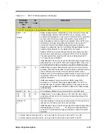
Table 2-10
C&T 65550 Pin Descriptions (continued)
Pin#
Pin Name
Type
Description
Flat Panel Display Interface (continued)
55
RSET
In
Set point resistor for the internal color palette DAC. A 560
Ω
1% resistor is required between RSET and AGND.
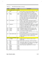
59
56
AVCC
AGND
VCC
GND
Analog power and ground pins for noise isolation for the
internal color palette DAC. AVCC should be isolated from
digital VCC as described in the Functional Description of the
internal color palette DAC. For proper DAC operation, AVCC
should not be greater than IVCC. AGND should be common
with digital ground but must be tightly decoupled to AVCC.
See the Functional Description of the internal color palette
DAC for further information .
203
XTALI (MCLK)
In
Crystal In. This pin .serves as the input for an external
reference oscillator (usually 14.31818 MHz). Note that in test
mode for the internal clock synthesizer, MCLK is output on
A25 (pin 30) and VCLK is output on A24 (pin
204
(Reserved)
Reserved. For compatibility with the 65545, this pin (formerly
"Crystal Out" or "XTLAO") must be disconnected. In addition,
pin 150 must be pulled down on reset. The 65545 no longer
supports the "internal oscillator option.
205
202
206
208
CVCC0
CGND0
CVCCI
CGNDI
VCC
GND
VCC
GND
Analog power and ground pins for noise isolation for the
internal clock synthesizer. Must be the same as VCC for
internal logic. VCC/GND pair 0 and VCC/GND pair 1 pins
must be carefully decoupled individually.
Note that the CVCC voltage must be the same as the voltage
for the internal logic (IVCC).
154
32KHz (GP102) (AA9)
In
Clock input for refresh of non-self-refresh DRAMs and panel
power sequencing. This pin can be programmed as GP102
instead of 32KHz input, or AA9 for 512Kx3 memory
configurations.
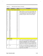
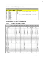
Power / Ground and Standby Control
178
STNDBY#
IN
Standby Control Pin. Pull this pin to place the chip in
Standby Mode.
80
77
181
184
IVCC
IGND
IVCC
IGND
VCC
GND
VCC
GND
Power / Ground (Internal Logic). 5V
±
10% or 3.3V
±
0.3V.
Note that this voltage must be the same as CVCC (voltage for
internal clock synthesizer). This voltage must also be equal
to, or greater than AVCC (voltage for DAC).
9
12
26
42
39
52
BVCC
BGND
BGND
BVCC
BGND
BGND
VCC
GND
GND
VCC
GND
GND
Power / Ground (Bus Interface) 5V
±
10% or 3.3V
±
0.3V.
Summary of Contents for Extensa 61X
Page 6: ...vi ...
Page 26: ...1 8 Service Guide Figure 1 5 Main Board Layout Bottom Side ...
Page 49: ...System Introduction 1 31 1 5 1 3 Power Management Figure 1 14 Power Management Block Diagram ...
Page 55: ...System Introduction 1 37 1 6 System Block Diagram Figure 1 15 System Block Diagram ...
Page 64: ...Major Chips Description 2 7 2 2 5 Pin Diagram Figure 2 4 M1521 Pin Diagram ...
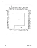
Page 99: ...2 42 Service Guide 2 5 3 Pin Diagram Figure 2 10 C T 65550 Pin Diagram ...
Page 117: ...2 60 Service Guide Figure 2 12 Functional block diagram CardBus Card Interface ...
Page 119: ...2 62 Service Guide Figure 2 14 PCI to CardBus terminal assignments ...
Page 135: ...2 78 Service Guide 2 7 3 Pin Diagram Figure 2 16 NS87336VJG Pin Diagram ...
Page 145: ...2 88 Service Guide 2 8 2 Pin Diagram Figure 2 17 YMF715 Block Diagram ...
Page 185: ...Disassembly and Unit Replacement 4 5 Figure 4 3 Disassembly Sequence Flowchart ...
Page 209: ...B 2 Service Guide ...
Page 210: ...Exploded View Diagram B 3 ...


