Major Chips Description
2-63
2.6.6
Terminal Functions
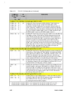
Table 2-13
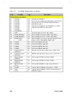
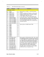
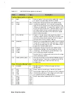
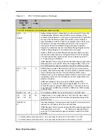
PCI1131 Pin Descriptions
TERMINAL
NAME NO.
I/O
TYPE
FUNCTION
PCI System Terminals
PCLK 165
I
PCI Bus clock. The PCI bus clock provides timing for all transactions on
the PCI bus. All PCI signals are sampled at the rising edge of PCLK.
RSTIN 166
I
PCI Reset. When the RSTIN signal is asserted low it causes the
PCI1131 to tri-state all output buffers and reset all internal registers.
When asserted, the 1131 device is completely nonfunctional. After
deasserting RSTIN, the PCI1131 is in its default state. When the 1131
SUSPEND mode is enabled, the device is protected from any RSTIn
reset (i.e., the 1131 internal register contents are preserved).
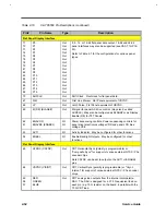
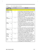
PCI Address and Data Terminals
AD31 170
AD30 171
AD29 173
AD28 174
AD27 176
AD26 177
AD25 178
AD24 179
AD23 183
AD22 184
AD21 185
AD20 186
AD19 188
AD18 189
AD17 190
AD16 191
AD15 204
AD14 205
AD13 206
AD12 208
AD11 1
AD10 2
AD9 3
AD8 4
AD7 6
AD6 8
AD5 9
AD4 10
AD3 11
AD2 12
AD1 14
AD0 15
I/O
Address/data bus. These signals are the multiplexed PCI address and
data bus. During the address phase of a PCI cycle, AD31-0 contain a 32-
bits address or other destination information. During the data phase,
AD31-0 contain data.
Summary of Contents for Extensa 61X
Page 6: ...vi ...
Page 26: ...1 8 Service Guide Figure 1 5 Main Board Layout Bottom Side ...
Page 49: ...System Introduction 1 31 1 5 1 3 Power Management Figure 1 14 Power Management Block Diagram ...
Page 55: ...System Introduction 1 37 1 6 System Block Diagram Figure 1 15 System Block Diagram ...
Page 64: ...Major Chips Description 2 7 2 2 5 Pin Diagram Figure 2 4 M1521 Pin Diagram ...
Page 99: ...2 42 Service Guide 2 5 3 Pin Diagram Figure 2 10 C T 65550 Pin Diagram ...
Page 117: ...2 60 Service Guide Figure 2 12 Functional block diagram CardBus Card Interface ...
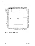
Page 119: ...2 62 Service Guide Figure 2 14 PCI to CardBus terminal assignments ...
Page 135: ...2 78 Service Guide 2 7 3 Pin Diagram Figure 2 16 NS87336VJG Pin Diagram ...
Page 145: ...2 88 Service Guide 2 8 2 Pin Diagram Figure 2 17 YMF715 Block Diagram ...
Page 185: ...Disassembly and Unit Replacement 4 5 Figure 4 3 Disassembly Sequence Flowchart ...
Page 209: ...B 2 Service Guide ...
Page 210: ...Exploded View Diagram B 3 ...


