2-66
Service Guide
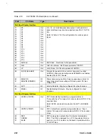
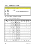
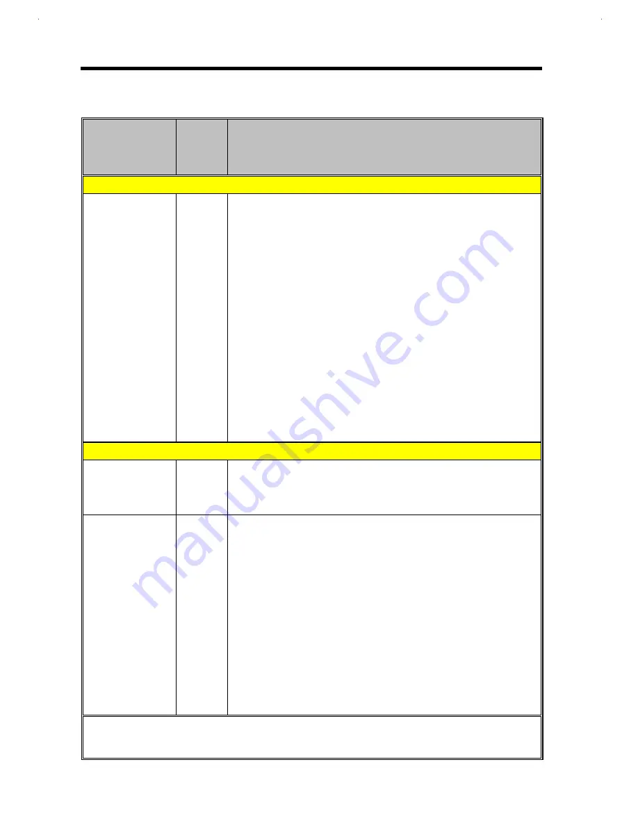
Table 2-13
PCI1131 Pin Descriptions (Continued)
TERMINAL
Name Slot
Slot
I/O
TYPE
FUNCTION
A+ B
≠≠
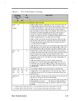
1 6-bit PC Card Address and Data (Slots A and B)
D15
93 27
D14
91 25
D13
89 23
D12
87 20
D11
84 18
D10
147 81
D9
145 79
D8
142 77
D6
90 24
D5
88 21
D4
85 19
D3
83 17
D2
146 80
D1
144 78
D0
141 76
I/O
PC Card Data. 16-bit PC Card data lines. D15 is the most significant
bit.
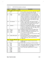
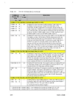
1 6-bit PC Card Interface Control Signals (Slots A and B)
CD1
82 16
CD2
140 74
I
PC Card Detect 1 and Card Detect 2. CD1 and CD2 are connected to
ground internally on the PC Card. When a PC Card is inserted into a
socket, these signals are pulled low. The signal status is available by
reading the Interface Status Register
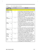
BVD1
(STSCHG/ 138
72
RI)
I
Battery Voltage Detect 1. Generated by 16-bit memory PC Cards that
include batteries. BVD1 is used with BVD2 as an indication of the
condition of the batteries on a memory PC Card. Both BVD1 and BVD2
are kept high when the battery is good. When BVD2 is low and BVD1 is
high, the battery is weak and needs to be replaced. When BVD1 is low,
the battery is no longer serviceable and the data in the memory PC
Card is lost. See the Card Status Change Interrupt Configuration
Register for enable bits (Section 8.6). See the Card Status Change
Register and the Interface Status Register for the status bits for this
signal.
Status Change. STSCHG is used to alert the system to a change in the
READY, Write Protect, or Battery Voltage Dead condition of a 16-bit I/O
PC Card.
Ring Indicate. RI is used by 1 6-bit modem cards to indicate ring
detection.
+
Terminal name is preceded with A_. As an example, the full name for terminal 121 is A_A25.
≠
Terminal name is preceded with B_. As an example, the full name for terminal 55 is B_A25.
Summary of Contents for Extensa 61X
Page 6: ...vi ...
Page 26: ...1 8 Service Guide Figure 1 5 Main Board Layout Bottom Side ...
Page 49: ...System Introduction 1 31 1 5 1 3 Power Management Figure 1 14 Power Management Block Diagram ...
Page 55: ...System Introduction 1 37 1 6 System Block Diagram Figure 1 15 System Block Diagram ...
Page 64: ...Major Chips Description 2 7 2 2 5 Pin Diagram Figure 2 4 M1521 Pin Diagram ...
Page 99: ...2 42 Service Guide 2 5 3 Pin Diagram Figure 2 10 C T 65550 Pin Diagram ...
Page 117: ...2 60 Service Guide Figure 2 12 Functional block diagram CardBus Card Interface ...
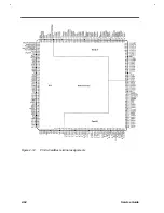
Page 119: ...2 62 Service Guide Figure 2 14 PCI to CardBus terminal assignments ...
Page 135: ...2 78 Service Guide 2 7 3 Pin Diagram Figure 2 16 NS87336VJG Pin Diagram ...
Page 145: ...2 88 Service Guide 2 8 2 Pin Diagram Figure 2 17 YMF715 Block Diagram ...
Page 185: ...Disassembly and Unit Replacement 4 5 Figure 4 3 Disassembly Sequence Flowchart ...
Page 209: ...B 2 Service Guide ...
Page 210: ...Exploded View Diagram B 3 ...

