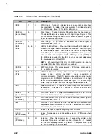
Major Chips Description
2-67
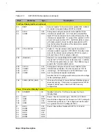
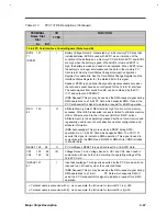
Table 2-13
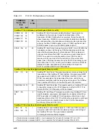
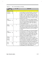
PCI1131 Pin Descriptions (Continued)
TERMINAL
Name Slot
Slot
I/O
TYPE
FUNCTION
A+ B
≠≠
1 6-bit PC Card Interface Control Signals (Slots A and B)
BVD2
137
71
(SPKR)
I
Battery Voltage Detect 2. Generated by 16-bit memory PC Cards that
include batteries. BVD2 is used with BVD 1 as an indication of the
condition of the batteries on a memory PC Card. Both BVD 1 and BVD2
are high when the battery is good. When BVD2 is low and BVD1 is
high, the battery is weak and needs to be replaced. When BVD1 is low,
the battery is no longer serviceable and the data in the memory PC
Card is lost. See the Card Status Change Interrupt Configuration
Register for enable bits. See the Card Status Change Register and the
Interface Status Register for the status bits for this signal
Speaker. SPKR is an optional binary audio signal available only when
the card and socket have been configured for the 16-bit l /O interface.
The audio signals from cards A and B can be combined by the PCI
1131 and output on SPKROUT.
(DMA Request) This pin may be used as the DMA request signal during
DMA operations to a 16-bit PC Card which supports DMA. If used, the
PC Card asserts this signal to indicate a request for a DMA operation.
REG
130
63
O
Attribute Memory Select. REG remains high for all common memory
accesses. When NES is asserted, access is limited to attribute memory
(OE or WE active) and to the l /O space (IORD or IOWR active).
Attribute memory is a separately accessed section of card memory and
is generally used to record card capacity and other configuration and
attribute information.
(DMA Acknowledge) This pin is used as a DACK during DMA
operations to a 1 6-bit PC Card which supports DMA. The PCI 1131
asserts this signal to indicate a DMA operation. This signal is used in
conjunction with the DMA Read (IOWR) or DMA Write (IORD) strobes
to transfer data.
RESET 124 58
O
PC Card Reset. RESET forces a hard reset to a 16-bit PC Card.
VS1 134 68
VS2 122 56
I/O
Voltage Sense 1 and Voltage Sense 2. VS1 and VS2, when used in
conjunction with each other, to determine the operating voltage of the
16-bit PC Card.
INPACK 127
61
I
Input Acknowledge. This signal is asserted by the PC Card when it can
respond to an l/O read cycle at the current address.
(DMA Request) This pin may be used as the DMA request signal during
DMA operations to a 16-bit
PC Card which supports DMA. If
used, the PC Card asserts this signal to indicate a request for a DMA
operation.
+
Terminal name is preceded with A_. As an example, the full name for terminal 121 is A_A25.
≠
Terminal name is preceded with B_. As an example, the full name for terminal 55 is B_A25.
Summary of Contents for Extensa 61X
Page 6: ...vi ...
Page 26: ...1 8 Service Guide Figure 1 5 Main Board Layout Bottom Side ...
Page 49: ...System Introduction 1 31 1 5 1 3 Power Management Figure 1 14 Power Management Block Diagram ...
Page 55: ...System Introduction 1 37 1 6 System Block Diagram Figure 1 15 System Block Diagram ...
Page 64: ...Major Chips Description 2 7 2 2 5 Pin Diagram Figure 2 4 M1521 Pin Diagram ...
Page 99: ...2 42 Service Guide 2 5 3 Pin Diagram Figure 2 10 C T 65550 Pin Diagram ...
Page 117: ...2 60 Service Guide Figure 2 12 Functional block diagram CardBus Card Interface ...
Page 119: ...2 62 Service Guide Figure 2 14 PCI to CardBus terminal assignments ...
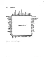
Page 135: ...2 78 Service Guide 2 7 3 Pin Diagram Figure 2 16 NS87336VJG Pin Diagram ...
Page 145: ...2 88 Service Guide 2 8 2 Pin Diagram Figure 2 17 YMF715 Block Diagram ...
Page 185: ...Disassembly and Unit Replacement 4 5 Figure 4 3 Disassembly Sequence Flowchart ...
Page 209: ...B 2 Service Guide ...
Page 210: ...Exploded View Diagram B 3 ...

