Major Chips Description
2-77
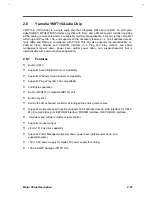
•
Plug and Play Compatible:
•
16 bit addressing(full programmable)
•
10 selectable IRQs
•
3 selectable DMA Channels
•
3 SIRQ Inputs allows external devices to mapping IRQs
•
100-Pin TQFP package - PC87336VJG
2.7.2
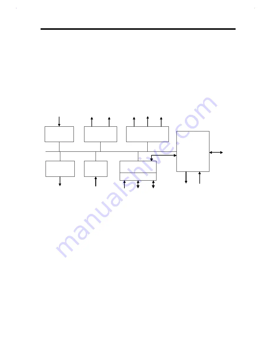
Block Diagram
Configuration
Registers
UART
(16550 or 16450)
UART
+ IrDA/HP & Sharp IR
(16550 or 16450)
General
Purpose
Registers
Power
Down Logic
IEEEE1284
Parallel Port
Hifh Current Driver
Floppy Disk
Controller with
Digital Data
Separator
(Enhabced 8477)
I/O Ports
Control
Interrupt
Data
Handshake
Floppy
Drive
Interface
OSC
Interrupt
and
DMA
Floppy
Drive
Interface
Interrupt
IR
Interface
Serial
Interface
Interrupt
Serial
Interface
Config.
Inputs
Figure 2-15
NS87336VJG Block Diagram
Summary of Contents for Extensa 61X
Page 6: ...vi ...
Page 26: ...1 8 Service Guide Figure 1 5 Main Board Layout Bottom Side ...
Page 49: ...System Introduction 1 31 1 5 1 3 Power Management Figure 1 14 Power Management Block Diagram ...
Page 55: ...System Introduction 1 37 1 6 System Block Diagram Figure 1 15 System Block Diagram ...
Page 64: ...Major Chips Description 2 7 2 2 5 Pin Diagram Figure 2 4 M1521 Pin Diagram ...
Page 99: ...2 42 Service Guide 2 5 3 Pin Diagram Figure 2 10 C T 65550 Pin Diagram ...
Page 117: ...2 60 Service Guide Figure 2 12 Functional block diagram CardBus Card Interface ...
Page 119: ...2 62 Service Guide Figure 2 14 PCI to CardBus terminal assignments ...
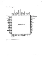
Page 135: ...2 78 Service Guide 2 7 3 Pin Diagram Figure 2 16 NS87336VJG Pin Diagram ...
Page 145: ...2 88 Service Guide 2 8 2 Pin Diagram Figure 2 17 YMF715 Block Diagram ...
Page 185: ...Disassembly and Unit Replacement 4 5 Figure 4 3 Disassembly Sequence Flowchart ...
Page 209: ...B 2 Service Guide ...
Page 210: ...Exploded View Diagram B 3 ...


