2-80
Service Guide
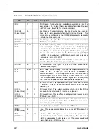
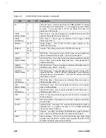
Table 2-14
NS87336VJG Pin Descriptions (continued)
Pin
No.
I/O
Description
/CS0,
/CS1
51, 3
O
Programmable Chip Select. /CS0, 1 are programmable chip select
and/or latch enable and/or output enable signals that can be used as
game port, I/O expand, etc. The decoded address and the assertion
conditions are configured via the 87336VJG’s configuration registers.
/CTS1,
/CTS2
72, 64
I
UARTs Clear to Send. When low, this indicates that the modem or
data set is ready to exchange data. The /CTS signal is a modem
status input. The CPU tests the condition of this /CTS signal by
reading bit 4 (CTS) of the Modem Status Register (MSR) for the
appropriate serial channel. Bit 4 is the complement of the CTS
signal. Bit 0 (DCTS) has no effect on the transmitter.
/CTS2 is multiplexed with A13. When it is not selected, it is masked
to “0”.
NOTE: Whenever the MSR DCTS bit is set, an interrupt is generated
if Modem Status interrupts are enabled.
D7-D0
10-17
I/O
Data. These are bidirectional data lines to the microprocessor. D0 is
the LSB and D7 is the MSB. These signals have a 24 mA (sink)
buffered outputs.
/DACK0
/DACK1
/DACK2
53,
52,
3
I
DMA Acknowledge 0, 1, 2. These active low inputs acknowledge the
DMA request and enable the /RD and /WR inputs during a DMA
transfer. It can be used by one of the following: FDC or Parallel Port.
If none of them uses this input pin, it is ignored. If the device which
uses on of this pins is disabled or configured with no DMA, this pin is
also ignored.
/DACK0, 1, 2should be held high during I/O accesses.
/DCD1, /DCD2
75, 67
I
UARTs Data Carrier Detect. When low, this indicates that the
modem or data set has detected the data carrier. The /DCD signal is
a modem status input. The CPU tests the condition of this /DCD
signal by reading bit 7 (DCD) of the Modem Status Register (MSR)
for the appropriate serial channel. Bit 7 is the complement of the
DCD signal. Bit 3 (DDCD) of the MSR indicates whether DCD input
has changed state since the previous reading of the MSR.
NOTE: Whenever the MSR DDCD bit is set, an interrupt is generated
if Modem Status interrupts are enabled.
Summary of Contents for Extensa 61X
Page 6: ...vi ...
Page 26: ...1 8 Service Guide Figure 1 5 Main Board Layout Bottom Side ...
Page 49: ...System Introduction 1 31 1 5 1 3 Power Management Figure 1 14 Power Management Block Diagram ...
Page 55: ...System Introduction 1 37 1 6 System Block Diagram Figure 1 15 System Block Diagram ...
Page 64: ...Major Chips Description 2 7 2 2 5 Pin Diagram Figure 2 4 M1521 Pin Diagram ...
Page 99: ...2 42 Service Guide 2 5 3 Pin Diagram Figure 2 10 C T 65550 Pin Diagram ...
Page 117: ...2 60 Service Guide Figure 2 12 Functional block diagram CardBus Card Interface ...
Page 119: ...2 62 Service Guide Figure 2 14 PCI to CardBus terminal assignments ...
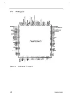
Page 135: ...2 78 Service Guide 2 7 3 Pin Diagram Figure 2 16 NS87336VJG Pin Diagram ...
Page 145: ...2 88 Service Guide 2 8 2 Pin Diagram Figure 2 17 YMF715 Block Diagram ...
Page 185: ...Disassembly and Unit Replacement 4 5 Figure 4 3 Disassembly Sequence Flowchart ...
Page 209: ...B 2 Service Guide ...
Page 210: ...Exploded View Diagram B 3 ...


