2-82
Service Guide
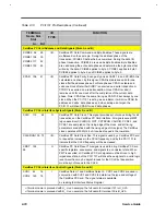
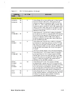
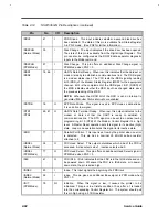
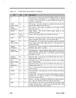
Table 2-14
NS87336VJG Pin Descriptions (continued)
Pin
No.
I/O
Description
/DRV2
47
I
FDD Drive2. This input indicates whether a second disk drive has
been installed. The state of this pin is available from Status Register
A in PS/2 mode. (See PNF for further information).
/DSKCHG
(Normal Mode)
30
I
Disk Change. The input indicates if the drive door has been opened.
The state of this pin is available from the Digital Input Register. This
pin can also be configured as the RGATE data separator diagnostic
input via the Mode command.
/DSKCHG
(PPM Mode)
87
I
Disk Change. This pin offers an additional Disk Change signal in
PPM Mode when PNF = 0.
/DSR1
/DSR2
74, 66
I
UARTs Data Set Ready. When low, this indicates that the data set or
modem is ready to establish a communications link. The DSR signal
is a modem status input. The CPU tests the /DSR signal by reading
bit 5 (DSR) of the Modem Status Register (MSR) for the appropriate
channel. Bit 5 is the complement of the DSR signal. Bit 1 (DDSR) of
the MSR indicates whether the DSR input has changed state since
the previous reading of the MSR.
NOTE: Whenever the DDSR bit of the NSR is set, an interrupt is
generated if Modem Status interrupts are enabled.
/DSTRB
76
O
EPP Data Strobe. This signal is used in EPP mode as data strobe.
It is an active low signal.
/DTR1
/DTR2
69, 61
O
UARTs Data Terminal Ready. When low, this output indicates to the
modem or data set that the UART is ready to establish a
communications link. The DTR signal can be set to an active low by
programming bit 0 (DTR) of the Modem Control Register to a high
level. A Master Reset operation sets this signal to its inactive (high)
state. Loop mode operation holds this signal to its inactive state.
/ERR
77
I
Parallel Port Error. This input is set low by the printer when an error
is detected. This pin has a nominal 25 KOHM pull-up resistor
attached to it.
/HDSEL
(Normal Mode)
32
O
FDC Head Select. This output determines which side of the FDD is
accessed. Active selects side 1, inactive selects side 0.
/HDSEL
(PPM Mode)
77
O
FDC Head Select. This pin offers an additional Head Select signal in
PPM Mode when PNF = 0.
IDLE
41
O
FDD IDLE. IDLE indicates that the FDC is in the IDLE state and can
be powered down. Whenever the FDC is in IDLE state, or in power-
down state, the pin is active high.
/INDEX
45
I
Index. This input signals the beginning of a FDD track.
/INDEX
(Normal Mode)
92
I
Index. This pin gives an additional Index signal in PPM mode when
PNF = 0.
/INIT
(PPM Mode)
78
I/O
Initialize. When this signal is low, it causes the printer to be
initialized. This pin is in a tristate condition 10 ns after a 1 is loaded
into the corresponding Control Register bit. The system should pull
this pin high using a 4.7 K
Ω
resistor.
Summary of Contents for Extensa 61X
Page 6: ...vi ...
Page 26: ...1 8 Service Guide Figure 1 5 Main Board Layout Bottom Side ...
Page 49: ...System Introduction 1 31 1 5 1 3 Power Management Figure 1 14 Power Management Block Diagram ...
Page 55: ...System Introduction 1 37 1 6 System Block Diagram Figure 1 15 System Block Diagram ...
Page 64: ...Major Chips Description 2 7 2 2 5 Pin Diagram Figure 2 4 M1521 Pin Diagram ...
Page 99: ...2 42 Service Guide 2 5 3 Pin Diagram Figure 2 10 C T 65550 Pin Diagram ...
Page 117: ...2 60 Service Guide Figure 2 12 Functional block diagram CardBus Card Interface ...
Page 119: ...2 62 Service Guide Figure 2 14 PCI to CardBus terminal assignments ...
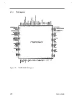
Page 135: ...2 78 Service Guide 2 7 3 Pin Diagram Figure 2 16 NS87336VJG Pin Diagram ...
Page 145: ...2 88 Service Guide 2 8 2 Pin Diagram Figure 2 17 YMF715 Block Diagram ...
Page 185: ...Disassembly and Unit Replacement 4 5 Figure 4 3 Disassembly Sequence Flowchart ...
Page 209: ...B 2 Service Guide ...
Page 210: ...Exploded View Diagram B 3 ...


