2-90
Service Guide
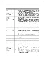
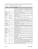
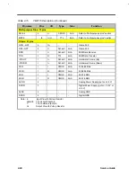
Table 2-15
YMF715 Descriptions (Continued)
Pin name
Pins
I/O
Type
Size
Function
Multi-purpose Dins: 13 pins
SEL2-0
3
I+
CMOS
2mA
Refer to “Multi-purpose pins” section
MP9-0
l0
I+/O
TTL
4mA
Refer to “multi-purpose pins” section
Others: 27 pins
GPO - GP3
4
IA
-
-
Game Port
GP4- GP7
4
I+
Schmitt
2mA
Game Port
RXD
1
I+
Schmitt
2rnA
MIDI Data Receive
TXD
1
O
TTL
4mA
MIDI Data Transfer
/VOLUP
1
I+
Schmitt
2mA
Hardware Volume (Up)
/VOLDW
l
I+
Schmitt
2mA
Hardware Volume (Down)
X331
1
I
CMOS
2mA
33.8688 MHz
X33O
1
O
CMOS
2mA
33.8688 MHz
X24I
1
I
CMOS
2mA
24.576 MHz
X24O
1
O
CMOS
2mA
24.576 MHz
AVDD
2
-
-
-
Analog Power Supply (put on +5.0V)
DVDD
3
-
-
-
Digital Power Supply (put on +5.0 V or
+3.3V)
AVSS
2
-
-
-
Analog GND
DVSS
4
-
-
-
Digital GND
Note: I+: Input Pin with Pull up Resistor
Schmitt: TTL-Schmitt input pin
T:
TTL-tri-state output pin
O+:
Output Pin with Pull up Resistor
Summary of Contents for Extensa 61X
Page 6: ...vi ...
Page 26: ...1 8 Service Guide Figure 1 5 Main Board Layout Bottom Side ...
Page 49: ...System Introduction 1 31 1 5 1 3 Power Management Figure 1 14 Power Management Block Diagram ...
Page 55: ...System Introduction 1 37 1 6 System Block Diagram Figure 1 15 System Block Diagram ...
Page 64: ...Major Chips Description 2 7 2 2 5 Pin Diagram Figure 2 4 M1521 Pin Diagram ...
Page 99: ...2 42 Service Guide 2 5 3 Pin Diagram Figure 2 10 C T 65550 Pin Diagram ...
Page 117: ...2 60 Service Guide Figure 2 12 Functional block diagram CardBus Card Interface ...
Page 119: ...2 62 Service Guide Figure 2 14 PCI to CardBus terminal assignments ...
Page 135: ...2 78 Service Guide 2 7 3 Pin Diagram Figure 2 16 NS87336VJG Pin Diagram ...
Page 145: ...2 88 Service Guide 2 8 2 Pin Diagram Figure 2 17 YMF715 Block Diagram ...
Page 185: ...Disassembly and Unit Replacement 4 5 Figure 4 3 Disassembly Sequence Flowchart ...
Page 209: ...B 2 Service Guide ...
Page 210: ...Exploded View Diagram B 3 ...


