BIOS Setup Information
3-9
The default setting is
[Standard and Bidirectional]
.
If you set EPP as the parallel port operation mode, do not use
3BCh as the parallel port base address; otherwise, I/O conflicts
may occur.
ECP DMA Channel
Set the ECP DMA Channel parameter if you set the Parallel Port Operation Mode to
[Enhanced
Capabilities Port(ECP)]
. The default value, with ECP selected, is
[0]
.
3.4.8
Passwords
Two passwords are implemented in this notebook. The Setup Password prevents unauthorized
access to the Setup utility, while the Power On Password prevents unauthorized access to the
notebook during boot-up and resume from hibernation.
Setting a Password
To set a password, select the desired password (Setup and Power On) to set or edit, and press
←
←
or
→
→
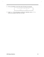
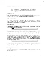
. The password prompt (a key) appears:
A message below the menu prompts you to enter a password. The password may consist of up to
seven characters which do not appear on the screen when you type them. After typing your
password, press Enter. Another prompt appears asking you to retype your password to verify your
first entry.
After setting a password, the notebook sets this parameter to
[Enabled]
. The next time you
boot the notebook, resume from hibernation mode or run the Setup utility, the password prompt
appears. Key in the appropriate password (Power On or Setup). If the password you entered is
incorrect, an “X” appears. You have three chances to type in the correct password. After three
tries, the following message appears:
Incorrect password specified. System disabled.
The notebook freezes up and disables all devices. You must turn off the notebook and turn it on
again to retry. If you forget your password, you must reset the configuration values stored in
CMOS to defaults. Resetting CMOS requires opening up the notebook, so contact your dealer for
assistance.
Removing a Password
To remove a password, select the desired password (Setup and Power On) to remove and press
←
←
or
→
→
to set it to
[None]
.
Summary of Contents for Extensa 61X
Page 6: ...vi ...
Page 26: ...1 8 Service Guide Figure 1 5 Main Board Layout Bottom Side ...
Page 49: ...System Introduction 1 31 1 5 1 3 Power Management Figure 1 14 Power Management Block Diagram ...
Page 55: ...System Introduction 1 37 1 6 System Block Diagram Figure 1 15 System Block Diagram ...
Page 64: ...Major Chips Description 2 7 2 2 5 Pin Diagram Figure 2 4 M1521 Pin Diagram ...
Page 99: ...2 42 Service Guide 2 5 3 Pin Diagram Figure 2 10 C T 65550 Pin Diagram ...
Page 117: ...2 60 Service Guide Figure 2 12 Functional block diagram CardBus Card Interface ...
Page 119: ...2 62 Service Guide Figure 2 14 PCI to CardBus terminal assignments ...
Page 135: ...2 78 Service Guide 2 7 3 Pin Diagram Figure 2 16 NS87336VJG Pin Diagram ...
Page 145: ...2 88 Service Guide 2 8 2 Pin Diagram Figure 2 17 YMF715 Block Diagram ...
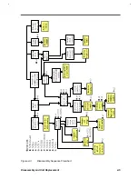
Page 185: ...Disassembly and Unit Replacement 4 5 Figure 4 3 Disassembly Sequence Flowchart ...
Page 209: ...B 2 Service Guide ...
Page 210: ...Exploded View Diagram B 3 ...


