System Introduction
1-
19
1.4.10
Video Memory
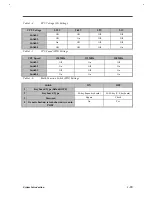
Table 1-15
Video RAM Configuration
Item
Specification
DRAM or VRAM
DRAM(EDO type)
Fixed or upgradeable
Fixed
Memory size/configuration
1MB (256K x 16 x 2pcs)
Memory speed
60ns
Memory voltage
3.3V
Memory package
TSOP
1.4.11
Video
Table 1-16
Video Hardware Specification
Item
Specification
Video chip
C&T65550B
Working voltage
C&T65550B: 3.3V
C&T65550XX: 3.3V/5V (“XX” represents codes other than “A” (i.e. “B1”))
Video Chip substitutability
Yes
During power-on, system supplies 5V to video chip and read its register to determine
whether the video chip is 5V or 3.3V/5V type. If 5V video chip is detected, system
maintains video voltage at 5V; if 3.3V/5V video chip is detected, system switches
video voltage to 3.3V.
1.4.11.1
External CRT Resolution Support
Table 1-17
Supported External CRT Resolutions
Resolution x Color on
External CRT
CRT Refresh Rate
Simultaneous on
TFT LCD
Simultaneous on
STN LCD
CRT only
Simultaneous
SVGA
SVGA
640x480x16
60,75,85
60
Y
Y
640x480x256
60,75,85
60
Y
Y
640x480x65,536
60,75,85
60
Y
Y
640x480x16,777,216
60,75,85
60
Y
N
800x600x16
56,60,75
60
Y
Y
800x600x256
56,60,75
60
Y
Y
800x600x65,536
56,60
60
Y
N
1024x768x16
60,75,86I
60
Y
Y
Table 1-17
Supported External CRT Resolutions (Continued)
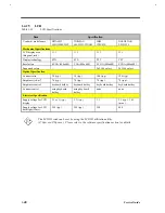
Resolution x Color on
External CRT
CRT Refresh Rate
Simultaneous on
TFT LCD
Simultaneous on
STN LCD
1024x768x256
60,75,86I
60
Y
Y
Summary of Contents for Extensa 61X
Page 6: ...vi ...
Page 26: ...1 8 Service Guide Figure 1 5 Main Board Layout Bottom Side ...
Page 49: ...System Introduction 1 31 1 5 1 3 Power Management Figure 1 14 Power Management Block Diagram ...
Page 55: ...System Introduction 1 37 1 6 System Block Diagram Figure 1 15 System Block Diagram ...
Page 64: ...Major Chips Description 2 7 2 2 5 Pin Diagram Figure 2 4 M1521 Pin Diagram ...
Page 99: ...2 42 Service Guide 2 5 3 Pin Diagram Figure 2 10 C T 65550 Pin Diagram ...
Page 117: ...2 60 Service Guide Figure 2 12 Functional block diagram CardBus Card Interface ...
Page 119: ...2 62 Service Guide Figure 2 14 PCI to CardBus terminal assignments ...
Page 135: ...2 78 Service Guide 2 7 3 Pin Diagram Figure 2 16 NS87336VJG Pin Diagram ...
Page 145: ...2 88 Service Guide 2 8 2 Pin Diagram Figure 2 17 YMF715 Block Diagram ...
Page 185: ...Disassembly and Unit Replacement 4 5 Figure 4 3 Disassembly Sequence Flowchart ...
Page 209: ...B 2 Service Guide ...
Page 210: ...Exploded View Diagram B 3 ...


