Major Chips Description
2-9
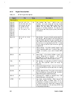
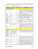
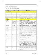
Table 2-2
M1521 Signal Descriptions (continued)
Signal
Pin
Type
Description
Host Interface
M/IOJ
H5
I
Host Memory or I/O. This bus definition pin
indicates the current bus cycle is either memory or
input/ output.
D/CJ
T7
I
Host Data or Code. This bus definition pin is used to
distinguish data access cycles from code access
cycles.
W/RJ
T9
I
Host Write or Read. When WRJ is driven high, it
indicates the current cycle is a write. Inversely, if
WRJ is driven low, a read cycle is performed.
HLOCKJ
G5
I
Host Lock. When HLOCKJ is asserted by the CPU,
the M1521 recognizes that the CPU is locking the
current cycles.
CACHEJ
J5
I
Host Cacheable. This pin is used to indicate the
host’s internal cacheability of the read cycles. If it is
driven inactive, the CPU does not cache the returned
data regardless of the state of KENJ.
KENJ/INV
K5
O
Cache Enable Output. This signal connects to the
CPU's KENJ and INV pins. KENJ is used to notify
the CPU whether the address of the current
transaction is cacheable. INV is used during L1
snoop cycles. The M1521 drives this signal high
(low) during the EADSJ assertion of a PCI master
write (read) snoop cycle.
SMIACTJ
T10
I
SMM Interrupt Active. It is asserted by the CPU to
inform the M1521 that SMM mode is being entered.
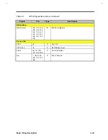
HD[63:0]
A1, B1, C3, C2, C1, D2,
D3, E3, D1, E2, E4, E1,
F3, F4, G3, F1, F2, H3,
G1, H4, G4, J3, G2,
H2, H1, J4, J1, J2, M4,
K1, M2, M3, N4, N2,
N3, P4, N1, P2, P3, R4,
P1, T2, R2, T4, R3, U2,
T3, U4, V2, U3, V4, T1,
W4, V3, W3, U1, R1,
V1, W2, W1, Y4, Y2,
Y3, Y1
I/O
Host Data Bus Lines. These signals connect to the
CPU's data bus.
DRAM Interface
MPD[7:0]
G18, H20, G20, H18,
F20, J18, G19, H19
I/O
DRAM Parity/ECC check bits. These are the 8-bit
parity/ECC check bits over DRAM bus.
RASJ[7] /
SRASJ[0]
N16
O
Row Address Strobe 7 or Synchronous DRAM RAS
0. FPM/EDO/BEDO of DRAM bank 7. SDRAM row
address strobe (SDRAM) copy 0.
Summary of Contents for Extensa 61X
Page 6: ...vi ...
Page 26: ...1 8 Service Guide Figure 1 5 Main Board Layout Bottom Side ...
Page 49: ...System Introduction 1 31 1 5 1 3 Power Management Figure 1 14 Power Management Block Diagram ...
Page 55: ...System Introduction 1 37 1 6 System Block Diagram Figure 1 15 System Block Diagram ...
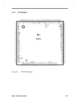
Page 64: ...Major Chips Description 2 7 2 2 5 Pin Diagram Figure 2 4 M1521 Pin Diagram ...
Page 99: ...2 42 Service Guide 2 5 3 Pin Diagram Figure 2 10 C T 65550 Pin Diagram ...
Page 117: ...2 60 Service Guide Figure 2 12 Functional block diagram CardBus Card Interface ...
Page 119: ...2 62 Service Guide Figure 2 14 PCI to CardBus terminal assignments ...
Page 135: ...2 78 Service Guide 2 7 3 Pin Diagram Figure 2 16 NS87336VJG Pin Diagram ...
Page 145: ...2 88 Service Guide 2 8 2 Pin Diagram Figure 2 17 YMF715 Block Diagram ...
Page 185: ...Disassembly and Unit Replacement 4 5 Figure 4 3 Disassembly Sequence Flowchart ...
Page 209: ...B 2 Service Guide ...
Page 210: ...Exploded View Diagram B 3 ...


