Major Chips Description
2-13
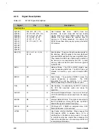
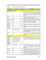
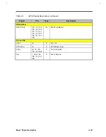
Table 2-2
M1521 Signal Descriptions (continued)
Signal
Pin
Type
Description
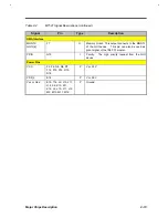
UMA Interface
MGNTJ/
GNTJ[4]
F7
O
Memory Grant. This output connects to the MGNTJ
of the GUI device. This pin can also be used as
grant signal of the fifth PCI master.
PRIO
G15
I
Priority. The high priority request from the GUI
device.
Power Pins
VCC
F5, F6, G6, R6, R7,
F14, F15, P15, R15,
R16
P
Vcc 3.3V
VDD_5
E14
P
Vcc 5.0V
Vss or Gnd
E15, T16, J9, J10, J11,
J12, K9, K10, K11,
K12, L9, L10, L11, L12,
M9, M10, M11, M12
P
Ground
Summary of Contents for Extensa 61X
Page 6: ...vi ...
Page 26: ...1 8 Service Guide Figure 1 5 Main Board Layout Bottom Side ...
Page 49: ...System Introduction 1 31 1 5 1 3 Power Management Figure 1 14 Power Management Block Diagram ...
Page 55: ...System Introduction 1 37 1 6 System Block Diagram Figure 1 15 System Block Diagram ...
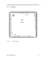
Page 64: ...Major Chips Description 2 7 2 2 5 Pin Diagram Figure 2 4 M1521 Pin Diagram ...
Page 99: ...2 42 Service Guide 2 5 3 Pin Diagram Figure 2 10 C T 65550 Pin Diagram ...
Page 117: ...2 60 Service Guide Figure 2 12 Functional block diagram CardBus Card Interface ...
Page 119: ...2 62 Service Guide Figure 2 14 PCI to CardBus terminal assignments ...
Page 135: ...2 78 Service Guide 2 7 3 Pin Diagram Figure 2 16 NS87336VJG Pin Diagram ...
Page 145: ...2 88 Service Guide 2 8 2 Pin Diagram Figure 2 17 YMF715 Block Diagram ...
Page 185: ...Disassembly and Unit Replacement 4 5 Figure 4 3 Disassembly Sequence Flowchart ...
Page 209: ...B 2 Service Guide ...
Page 210: ...Exploded View Diagram B 3 ...

