Major Chips Description
2-19
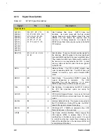
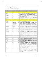
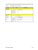
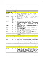
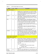
Table 2-3
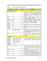
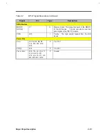
M1523 Signal Descriptions (continued)
Signal
Pin
Type
Description
PCI Interrupt Unit
INTAJ_MI
67
I
PCI Interrupt Input A or PCI interrupt polling input.
INTBJ
68
I/O
PCI Interrupt Input B or polling select_0 output.
INTCJ
69
I/O
PCI Interrupt Input C or polling select_1 output.
INTDJ
70
I/O
PCI Interrupt Input D or polling select_2 output.
PCI Arbiter
PHOLDJ
66
O
M1523 requests the ownership of the PCI bus.
Hardware setting option
Pull low : internal RTC is enabled
Pull high : external RTC is used.
PHLDAJ
65
I
PCI Hold Acknowledge. When this pin is asserted, the
M1523 owns the PCI bus.
CPU Interface (3.3V)
IGNNEJ
55
O
Ignore Numeric Error. This pin is used as the ignore
numeric coprocessor error.
INTR
54
O
Interrupt Request to CPU. This is the interrupt signal
generated by the internal 8259.
NMI
58
O
Non-maskable Interrupt. This is non-maskable interrupt
request to CPU.
A20MJ
56
O
CPU A20 Mask. This is the address line 20 mask signal.
ISA Interface
FERRJ/IRQ13
62
I
Floating Point Error. FERRJ input to generate IRQ13.
When the coprocessor interface is disabled in
configuration port 43h bit 6, the function of this pin is
IRQ13.
IRQ12 / MDATAO
155
I/O
Mouse Interrupt Request Input/Mouse Data Output. When
internal PS/2 keyboard is disabled, this pin is mouse
interrupt input. Otherwise, this pin is mouse data output.
IRQ[15:14],
IRQ[11:9],
IRQ[7:3]
20, 22, 13, 11,
164, 194, 196,
200, 202
I
Interrupt Request Signals.
SD[15:8]
42, 41, 39, 37,
35, 33, 31, 29
I/O
ISA High-byte Slot Data Bus. These lines are system data
lines.
XD[7:0]
161-163, 165,
167, 168, 170-
171
I/O
External Data Bus lines connect to SD[7:0] by an external
TTL LS245, whose direction is controlled by the M1523
output signal XDIR.
SA19
175
O
ISA Slot Address Bus A19.
SA18
177
O
ISA Slot Address Bus A18.
SA17
179
O
ISA Slot Address Bus A17.
Summary of Contents for Extensa 61X
Page 6: ...vi ...
Page 26: ...1 8 Service Guide Figure 1 5 Main Board Layout Bottom Side ...
Page 49: ...System Introduction 1 31 1 5 1 3 Power Management Figure 1 14 Power Management Block Diagram ...
Page 55: ...System Introduction 1 37 1 6 System Block Diagram Figure 1 15 System Block Diagram ...
Page 64: ...Major Chips Description 2 7 2 2 5 Pin Diagram Figure 2 4 M1521 Pin Diagram ...
Page 99: ...2 42 Service Guide 2 5 3 Pin Diagram Figure 2 10 C T 65550 Pin Diagram ...
Page 117: ...2 60 Service Guide Figure 2 12 Functional block diagram CardBus Card Interface ...
Page 119: ...2 62 Service Guide Figure 2 14 PCI to CardBus terminal assignments ...
Page 135: ...2 78 Service Guide 2 7 3 Pin Diagram Figure 2 16 NS87336VJG Pin Diagram ...
Page 145: ...2 88 Service Guide 2 8 2 Pin Diagram Figure 2 17 YMF715 Block Diagram ...
Page 185: ...Disassembly and Unit Replacement 4 5 Figure 4 3 Disassembly Sequence Flowchart ...
Page 209: ...B 2 Service Guide ...
Page 210: ...Exploded View Diagram B 3 ...


