2-26
Service Guide
2.4.3
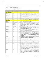
Pin Description
Table 2-4
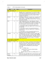
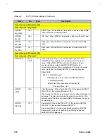
M7101 Pin Descriptions
Name
No.
Type
Description
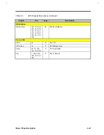
PCI interface : (42)
PCICLK
89
I
PCI Clock. This is the PCI Bus interface CLK input signal. This
clock frequency should not be more than 33 Mhz. It is used by
internal PCI interface.
AD[31:0]
91-98,2-
9, 20-
25, 27,
28, 30-
37
I/O
PCI Address and Data bus. These lines are connected to PCI Bus’
AD[31:0]. These lines contain Address and Data bus information
for PCI transaction.
CBEJ[3:0]
99,10,
17,29
I
PCI Bus Command and Byte enable. These are PCI bus
commands at address phase and byte enable signals at data phase.
Since M7101 is PCI slave only, it will not drive CBEJ[3:0]. They are
inputs only.
FRAMEJ
12
I
Cycle FRAME for PCI bus. This signal indicates the beginning and
duration of a PCI access.
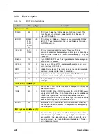
DEVSELJ
15
O
Device select. When M7101 has decoded the address as its own
cycle, it will assert DEVSELJ.
IRDYJ
13
I
Initiator Device Ready. This signal indicates the initiator is ready to
complete the current data phase of transaction.
TRDYJ
14
O
Target Device Ready. This signal indicates that M7101 is ready to
complete the current data phase of transaction.
PAR
16
O
Parity bit of PCI bus. It is the even parity bit across AD[31:0] and
CBEJ[3:0]
CLK & RESET interface : (3)
CLK32
62
I
32KHz clock. This is 32KHz clock input, used by internal timers and
relative PMU circuit.
PWGD
40
I
POWER GOOD. When PWGD low means the VDD5&VDD3 power
supply is turned off. When high, it means the power is available and
stable. This signal will be sent to suspend circuit to disable the
suspend protected circuit when PWGD is high. It will also be sent to
reset the circuit supplied by VDD5&VDD3 power.
SUSRSTJ
39
I
SUSPEND RESET. SUSPEND circuit RESET signal. When low,
the suspend circuit will be reset. The suspend circuit is supplied by
the VDDS power.
PMU Input event interface : (11)
ACPWR
49
I
AC power. When plugged in or out, the AC adapter status will be
reflected at this signal. Both low to high or high to low transition will
generate SMIJ. An internal debounce is built-in to avoid the input
bouncing problem. Both rising & falling will be detected. This is a
smith-trigger input signal.
Summary of Contents for Extensa 61X
Page 6: ...vi ...
Page 26: ...1 8 Service Guide Figure 1 5 Main Board Layout Bottom Side ...
Page 49: ...System Introduction 1 31 1 5 1 3 Power Management Figure 1 14 Power Management Block Diagram ...
Page 55: ...System Introduction 1 37 1 6 System Block Diagram Figure 1 15 System Block Diagram ...
Page 64: ...Major Chips Description 2 7 2 2 5 Pin Diagram Figure 2 4 M1521 Pin Diagram ...
Page 99: ...2 42 Service Guide 2 5 3 Pin Diagram Figure 2 10 C T 65550 Pin Diagram ...
Page 117: ...2 60 Service Guide Figure 2 12 Functional block diagram CardBus Card Interface ...
Page 119: ...2 62 Service Guide Figure 2 14 PCI to CardBus terminal assignments ...
Page 135: ...2 78 Service Guide 2 7 3 Pin Diagram Figure 2 16 NS87336VJG Pin Diagram ...
Page 145: ...2 88 Service Guide 2 8 2 Pin Diagram Figure 2 17 YMF715 Block Diagram ...
Page 185: ...Disassembly and Unit Replacement 4 5 Figure 4 3 Disassembly Sequence Flowchart ...
Page 209: ...B 2 Service Guide ...
Page 210: ...Exploded View Diagram B 3 ...


