Major Chips Description
2-29
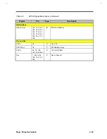
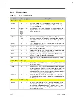
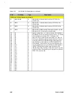
Table 2-4
M7101 Pin Descriptions (Continued)
Name
No.
Type
Description
PMU output interface (9)
CCFT
57
O
Backlight control. This signal is used to turn on/off LCD backlight.
FPVEE will AND with offset 0D2h D0 to generate CCFT. That is, if
both FPVEE and offset 0D2h D0 are high then CCFT will be high or
1Khz signal with programmed duty cycle by offset 0Fbh D[4:0].
Otherwise CCFT will be low.
DISPLAY
58
O
LCD Display On/Off control. This signal is used to control the LCD
display ON/OFF. If FPVEE goes from low to high, DISPLAY will
also go high after a period of about 62.5ms to 125ms. If not active,
it will go low immediately.
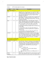
SMIJ
18
O
System Management Interrupt. System Management interrupt
output. It is the SMIJ output when internal SMIJ is generated or the
IN_SMIJ input of the APM function is asserted. The high/low active
level can be selected. There are three types of active method :
1. If offset 0D2h D7=1,D3=0, this signal will be asserted until
reading/writing all of SMIJ status register‘s bits. This can be treated
as a level SMIJ.
2. If offset 0D2h D7=0, D3=1, this signal will be asserted until
reading/writing all of SMIJ status register‘s bits or a programmed
interval time out.
3. If offset 0D2h D7=0, D3=0, this signal will be asserted for an
interval time. This can be treated as a pulse SMIJ.
SUSTATE
45
O
SUSPEND STATE. When writing to port 0FAh or POSSTA goes
high, the SUSTATE will go high. The system will enter SUSPEND
mode. Only VDDS will supply the power, other VDD5 or VDD3 will
have no power. Only RI, RTC, HOTKEYJ or COVSW can wake up
the system and let the SUSTATE be low again. The VDD5 and
VDD3 will supply power.
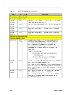
General purpose I/O interface(24)
General purpose I/O group A
GPIOA[7:0]
71-64
I/O
General Purpose I/O group A. These signals can be programmed to
be inputs or outputs. Offset 0D9h D[7:0] control the I/O attributes.
When programmed to be outputs, offset 0D8h D[7:0] will be set to
corresponding signal. When programmed to be inputs, the signal
can be read from the Offset 0D8h D[7:0] corresponding bits.
Offset 0D9h
D[n] = 0 GPIOA[n]= Input
GPIOA[n] value can be read from Offset 0D8h D[n]
1 GPIOA[n]= Output
Offset 0D8h D[n] value will be sent to GPIOA[n] where "n" is
from 7 to 0
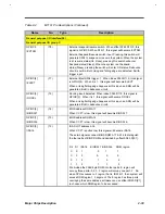
GPIOA7
/POSSTA
(71)
I
Positive input. When offset 0F6h D13=‘1’, this pin will sense a high
level to active SUSTATE pin and force M7101 input suspend mode.
Summary of Contents for Extensa 61X
Page 6: ...vi ...
Page 26: ...1 8 Service Guide Figure 1 5 Main Board Layout Bottom Side ...
Page 49: ...System Introduction 1 31 1 5 1 3 Power Management Figure 1 14 Power Management Block Diagram ...
Page 55: ...System Introduction 1 37 1 6 System Block Diagram Figure 1 15 System Block Diagram ...
Page 64: ...Major Chips Description 2 7 2 2 5 Pin Diagram Figure 2 4 M1521 Pin Diagram ...
Page 99: ...2 42 Service Guide 2 5 3 Pin Diagram Figure 2 10 C T 65550 Pin Diagram ...
Page 117: ...2 60 Service Guide Figure 2 12 Functional block diagram CardBus Card Interface ...
Page 119: ...2 62 Service Guide Figure 2 14 PCI to CardBus terminal assignments ...
Page 135: ...2 78 Service Guide 2 7 3 Pin Diagram Figure 2 16 NS87336VJG Pin Diagram ...
Page 145: ...2 88 Service Guide 2 8 2 Pin Diagram Figure 2 17 YMF715 Block Diagram ...
Page 185: ...Disassembly and Unit Replacement 4 5 Figure 4 3 Disassembly Sequence Flowchart ...
Page 209: ...B 2 Service Guide ...
Page 210: ...Exploded View Diagram B 3 ...


