Major Chips Description
2-31
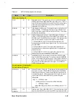
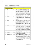
Table 2-4
M7101 Pin Descriptions (Continued)
Name
No.
Type
Description
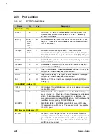
General purpose I/O interface(24)
General purpose I/O group A
GPIOA0
/GPIORAJ
(64)
O
External General Purpose I/O A read. When SPKCTL is pull low
4.7K, the GPIOA0 will become GPIORAJ. External General
purpose A Read control pulse, When Read index 0E1h with a byte
or a word. A 74245 OEJ pulse will be generated at this pin. The
74245 output should be connected to PCI AD[23:16] if a byte
command. If a word command, two 74245s will be used and
outputs are connected to PCI AD[31:16]. When read index 0E1h,
M7101 will send DEVSELJ, TRDYJ but float the AD[31:0] because
the data will be sent by 74245. The write action has no meaning
and nothing will be done.
General purpose I/O interface(24)
General purpose I/O group B
GPIOB[7 :0]
88,85,
87,86,
84-81
I/O
General Purpose I/O group B. These signals can be programmed to
be input or output. Offset 0DBh D[7:0] control the I/O attribute.
When programmed to be output, Offset 0DAh D[7:0] will set to
corresponding signal. When programmed to be input, the signal
can be read from the Offset 0DAh D[7:0] corresponding bits.
Offset 0DBh
D[n] = 0 : GPIOB[n]=input
GPIOB[n] value can be read from Offset 0DAh D[n]
1 : GPIOB[n]=Output
Offset 0DAh D[n] value will send to GPIOB[n]
"n" value is from 7 to 0
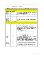
GPIOB7
/STPCLKJ
(88)
O
Stop clock signal. When DISPLAY is pulled low or offset 0F6h
D14=‘1’, this pin will become stop clock signal output. It may be
connected to CPU to force it into STPGNT or STPCLK mode. Write
port 0EFh will assert this function.
GPIOB6
/AMSTATJ
(85)
O
APM State. When DISPLAY is pulled low, this pin will be APM state.
It may be connected to clock generator to slow down clock. It is
asserted when HALT or STPGNT cycle is detected and recovers
when IN_SMIJ, IN_INTR or IN_INIT is asserted. System can use
this signal to know the APM status, and slow down the speed or turn
off some peripheral power to decrease the power consumption.
This signal will be synchronized with PCICLK‘s rising or falling edge.
GPIOB5
/OUT_INIT
(87)
O
INIT Output. When DISPLAY is pulled low, this pin will be INIT
output. It will be disabled when IN_INIT is detected and AMSTATJ is
asserted. Then, it will be sent as a 16 PCICLK wide pulse after
AMSTATJ is deasserted. Otherwise, it will be the same with
IN_INIT. It may be connected to CPU.
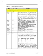
GPIOB4
/OUT_INTR
(86)
O
INTR Output. When DISPLAY is pulled low, this pin will become
INTR output. It may be connected to CPU. When AMSTATJ is
asserted, IN_INTR will be masked until AMSTATJ is de-asserted.
Summary of Contents for Extensa 61X
Page 6: ...vi ...
Page 26: ...1 8 Service Guide Figure 1 5 Main Board Layout Bottom Side ...
Page 49: ...System Introduction 1 31 1 5 1 3 Power Management Figure 1 14 Power Management Block Diagram ...
Page 55: ...System Introduction 1 37 1 6 System Block Diagram Figure 1 15 System Block Diagram ...
Page 64: ...Major Chips Description 2 7 2 2 5 Pin Diagram Figure 2 4 M1521 Pin Diagram ...
Page 99: ...2 42 Service Guide 2 5 3 Pin Diagram Figure 2 10 C T 65550 Pin Diagram ...
Page 117: ...2 60 Service Guide Figure 2 12 Functional block diagram CardBus Card Interface ...
Page 119: ...2 62 Service Guide Figure 2 14 PCI to CardBus terminal assignments ...
Page 135: ...2 78 Service Guide 2 7 3 Pin Diagram Figure 2 16 NS87336VJG Pin Diagram ...
Page 145: ...2 88 Service Guide 2 8 2 Pin Diagram Figure 2 17 YMF715 Block Diagram ...
Page 185: ...Disassembly and Unit Replacement 4 5 Figure 4 3 Disassembly Sequence Flowchart ...
Page 209: ...B 2 Service Guide ...
Page 210: ...Exploded View Diagram B 3 ...

