2-34
Service Guide
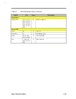
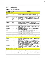
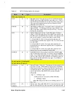
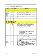
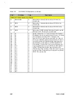
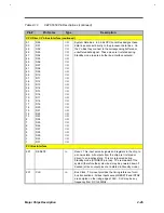
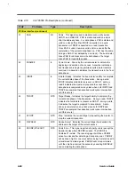
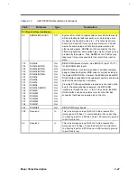
Table 2-4
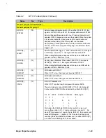
M7101 Pin Descriptions (Continued)
Name
No.
Type
Description
Power Pins
VDD5 x 3
11,59,76
P
5V VDD input
VDD3 x 2
26,100
P
3.3V VDD input
VDDS x 1
46
P
5V Suspend VDD input. This pin supplies to RI, RTC, HOTKEYJ,
COVSW, SUSTATE, PWGD, SUSRSTJ pad.
VSS x 5
1,19,38,
63,90
P
VSS Ground.
2.4.4
Different Pin definition setting
•
SLED, CCFT, DISPLAY, SPKCTL, SQWO and GPIOC2 pins are all internal pull high 50K
ohms. The blank part of following table means keeping the original pin definition.
•
When SLED default is pulled high, the chip will be in normal mode.
•
When SLED is pulled low by 4.7K resistor, the chip will be in test mode.
•
When GPIOC2 pull low, the PCI ports are 0078/007A and offset 0F6h D15 will be set, otherwise,
0178/017A.
Table 2-5
M7101 Different Pin Definition Setting
Original pin
definition
CCFT
pull low 4.7K
DISPLAY
pull low 4.7K
SPKCTL
pull low 4.7K
SQWO
pull low 4.7K
offset 0F6h D1=1
offset 0F6h D2=1
offset 0F6h D3=1
offset 0F6h D4=1
GPIOA5
GPIOWB
GPIOA4
GPIORBJ
GPIOA1
GPIOWA
GPIOA0
GPIORAJ
GPIOB7
STPCLKJ
GPIOB6
AMSTATJ
GPIOB5
OUT_INIT
GPIOB4
OUT_INTR
GPIOB3
IN_BRDYJ
GPIOB2
IN_INIT
GPIOB1
IN_SMIJ
GPIOB0
IN_INTR
GPIOC2
BIOSA17
GPIOC1
BIOSA16
GPIOC0
ISA16
Summary of Contents for Extensa 61X
Page 6: ...vi ...
Page 26: ...1 8 Service Guide Figure 1 5 Main Board Layout Bottom Side ...
Page 49: ...System Introduction 1 31 1 5 1 3 Power Management Figure 1 14 Power Management Block Diagram ...
Page 55: ...System Introduction 1 37 1 6 System Block Diagram Figure 1 15 System Block Diagram ...
Page 64: ...Major Chips Description 2 7 2 2 5 Pin Diagram Figure 2 4 M1521 Pin Diagram ...
Page 99: ...2 42 Service Guide 2 5 3 Pin Diagram Figure 2 10 C T 65550 Pin Diagram ...
Page 117: ...2 60 Service Guide Figure 2 12 Functional block diagram CardBus Card Interface ...
Page 119: ...2 62 Service Guide Figure 2 14 PCI to CardBus terminal assignments ...
Page 135: ...2 78 Service Guide 2 7 3 Pin Diagram Figure 2 16 NS87336VJG Pin Diagram ...
Page 145: ...2 88 Service Guide 2 8 2 Pin Diagram Figure 2 17 YMF715 Block Diagram ...
Page 185: ...Disassembly and Unit Replacement 4 5 Figure 4 3 Disassembly Sequence Flowchart ...
Page 209: ...B 2 Service Guide ...
Page 210: ...Exploded View Diagram B 3 ...


