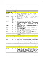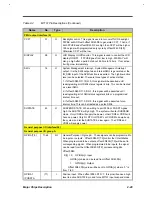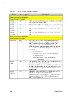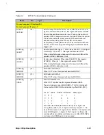
Major Chips Description
2-39
Table 2-9
M7101 PCI Interface Lock Register
Action
I/O Port
0178h/0078h
I/O Port 017Ah/007Ah
Lock Read
not available
except offset
0D1h
not available except offset 0D1h
Lock Write
not available
except offset
0D1h
not available except offset 0D1h
Unlock
Read
available
available
Unlock
Write
available
available
State Machine for PCI Interface.
FRAMEJ='1'
IDLE
nocycle='1', when FRAMEJ='1' and IRDYJ='1'.
='0', when others.
HIT='1', when read/write port 178-17B.
='0', when others.
FRAMEJ='1'
FRAMEJ='0'
IRDYJ='0'
IRDYJ='1'
HIT='0'
nocycle='0' and
nocycle='0' and
HIT='1'
HIT='0' and
FRAMEJ='1'
nocycle='1' or
FRAMEJ='0'
BUS_BUSY
TURN_AR
OVER_S
HITCMD3
HITCMD2
HITCMD
1
START_S
Figure 2-8
State Machine for PCI Interface
Summary of Contents for Extensa 61X
Page 6: ...vi ...
Page 26: ...1 8 Service Guide Figure 1 5 Main Board Layout Bottom Side ...
Page 49: ...System Introduction 1 31 1 5 1 3 Power Management Figure 1 14 Power Management Block Diagram ...
Page 55: ...System Introduction 1 37 1 6 System Block Diagram Figure 1 15 System Block Diagram ...
Page 64: ...Major Chips Description 2 7 2 2 5 Pin Diagram Figure 2 4 M1521 Pin Diagram ...
Page 99: ...2 42 Service Guide 2 5 3 Pin Diagram Figure 2 10 C T 65550 Pin Diagram ...
Page 117: ...2 60 Service Guide Figure 2 12 Functional block diagram CardBus Card Interface ...
Page 119: ...2 62 Service Guide Figure 2 14 PCI to CardBus terminal assignments ...
Page 135: ...2 78 Service Guide 2 7 3 Pin Diagram Figure 2 16 NS87336VJG Pin Diagram ...
Page 145: ...2 88 Service Guide 2 8 2 Pin Diagram Figure 2 17 YMF715 Block Diagram ...
Page 185: ...Disassembly and Unit Replacement 4 5 Figure 4 3 Disassembly Sequence Flowchart ...
Page 209: ...B 2 Service Guide ...
Page 210: ...Exploded View Diagram B 3 ...


