Major Chips Description
2-95
2.9.6
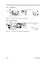
Pin Description
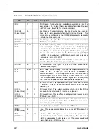
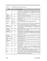
Table 2-18
T62.062.C Pin Description table
Item
Pin Name
I/O
Description
SAFETY OPERATION
1
DC_BAT_OUT
O/P
.adapter power input and battery power output terminal(
with 5 A short circuit protection)
2
DC_BAT_OUT
O/P
same as pin 1
3
DC_BAT_OUT
O/P
same as pin 1
4
DC_BAT_OUT
O/P
same as pin 1
5
GND
ground
6
GND
ground
7
PERIPHERAL
SYSTEM ON
I/P
system power on ,input a high pulse. user have different
way to turn on sysem by peripheral device.
8
5VSB_OUT
O/P
charger 5VSB output
9
SYSTEM ON
O/P
connecting to main system ‘power on ’ signal
10
DISABLE
I/P
logic high to notice charger to turn off system
11
BT-QCHG
O/P
charge status, when quick charge output logic high.
12
AD5V
O/P
when adapter inserted, 5V,10mA (max).
13
SMI
O/P
open collector, when push power on switch then output
low. (delay 6040 mS)
14
S.I.U.
I/P
logic high when system in use power
15
TH
I/P
connecting to thermistor inside battery pack using 103AT-
2 (10K/25,1%).
16
BL1#
O/P
when battery voltage lower than BL1 voltage then output
low (available when S.I.U).
17
ID
I/P
open circuit when a 9 cells LIB battery inserted,
connecting to GND when a 9 cells NiMH battery inserted.
18
BL2#
O/P
when battery voltage lower than BL2 voltage then output
low (available when S.I.U).
19
GND.
.
20
BAT-IN-USE#
O/P
logic low when battery in use power
(available when S.I.U).
21
BT_VS
I/P
connecting to battery most positive terminal
22
GND
23
BT+
I/O
connecting to battery most positive terminal
24
BT+
I/O
same as pin 23
25
BT+
I/O
same as pin 23
26
BT+
I/O
same as pin 23
Summary of Contents for Extensa 61X
Page 6: ...vi ...
Page 26: ...1 8 Service Guide Figure 1 5 Main Board Layout Bottom Side ...
Page 49: ...System Introduction 1 31 1 5 1 3 Power Management Figure 1 14 Power Management Block Diagram ...
Page 55: ...System Introduction 1 37 1 6 System Block Diagram Figure 1 15 System Block Diagram ...
Page 64: ...Major Chips Description 2 7 2 2 5 Pin Diagram Figure 2 4 M1521 Pin Diagram ...
Page 99: ...2 42 Service Guide 2 5 3 Pin Diagram Figure 2 10 C T 65550 Pin Diagram ...
Page 117: ...2 60 Service Guide Figure 2 12 Functional block diagram CardBus Card Interface ...
Page 119: ...2 62 Service Guide Figure 2 14 PCI to CardBus terminal assignments ...
Page 135: ...2 78 Service Guide 2 7 3 Pin Diagram Figure 2 16 NS87336VJG Pin Diagram ...
Page 145: ...2 88 Service Guide 2 8 2 Pin Diagram Figure 2 17 YMF715 Block Diagram ...
Page 185: ...Disassembly and Unit Replacement 4 5 Figure 4 3 Disassembly Sequence Flowchart ...
Page 209: ...B 2 Service Guide ...
Page 210: ...Exploded View Diagram B 3 ...


