background image


Theory of Operation


 4-15


functions. All popular 5.25-inch and 3.5-inch floppy disk drives, including the 2.88 MB, 
3.5-inch floppy disk drive, are supported. In addition, automatic media sense and 
2 Mbps tape drive support are provided by the FDC.

The two UARTs are fully NS16450 and NS16550 compatible. Both ports support MIDI 
baud rates and one port also supports IrDA 1.0 SIR (with data rate of 115.2 Kbps), IrDA 
1.1 MIR and FIR (with data rate of 1.152 Mbps and 4.0 Mbps respectively), and Sharp 
SIR (with data rate of 38.4 Kbps respectively) compliant signaling protocol.

The parallel port is fully IEEE 1284 level 2 compatible. The SPP (Standard Parallel Port) 
is fully compatible with ISA and EISA parallel ports. In addition to the SPP, EPP 
(Enhanced Parallel Port) and ECP (Extended Capabilities Port) modes are supported by 
the parallel port.

A set of configuration registers are provided to control the Plug and Play and other 
various functions of the PC87338. These registers are accessed using two 8-bit wide 
index and data registers. The ISA I/O address of the register pair can be relocated using 
a power-up strapping option and the software configuration after power-up.

When idle, advanced power management features allows the PC87338 to enter 
extremely low power modes under software control. The PC87338 operates at a 3.3/5V 
power supply.

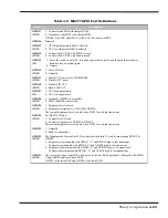
4.2.7.1.1 PC87338 Features

100% compatible with ISA, and EISA architectures

Floppy Disk Controller

Software compatible with the DP8473, the 765A and the N82077

16-byte FlFO (disabled by default)

Burst and Non-Burst modes

Perpendicular Recording drive support

New high-performance internal digital data separator (no external filter 
components required)

Low-power CMOS with enhanced power-down mode

Automatic media-sense support, with full IBM TDR (Tape Drive Register) 
implementation

Supports fast 2 Mbps and standard 1 Mbps/500 kbps/250 kbps tape drives

Bidirectional Parallel Port

Enhanced Parallel Port (EPP) compatible

Summary of Contents for Extensa 900 Series

Page 1: ...Maintenance Manual ExtensaTM 900 Series Notebook Computers 9813715 0001 December 1996 ...

Page 2: ...r her business Address all correspondence regarding orders to Texas Instruments P O Box 6102 M S 3255 Temple Texas 76503 Extensa is a trademark of Texas Instruments The icons in the Windows Notebook and Startup groups are copyrighted by Texas Instruments IBM and PS 2 are registered trademarks and OS 2 is a trademark of International Business Machines Corporation Microsoft Windows and MS DOS are re...

Page 3: ...on Describes how to unpack install options and begin using the notebook Section 3 Operating Instructions Describes the notebook computer operating controls and indicators and basic operating procedures required to support maintenance operations Section 4 Theory of Operation Provides a block diagram level theory of operation for the Extensa Series Notebooks Section 5 Troubleshooting Procedures Prov...

Page 4: ...eries Notebook Computers Users Guide Contains user reference information for the Extensa 900 Series Notebook Computers PC Doctor Help and Technical Reference online Ordering Parts and Supplies To order a copy of any TI publication or to order option kits spare parts or supplies for your system contact your TI reseller Telephone Toll free 1 800 TI TEXAS ...

Page 5: ...ivity Features 1 5 Notebook Expansion Capabilities 1 7 Memory Expanson 1 7 PCMCIA Card Options 1 7 Mobile Productivity Base Option 1 7 Docking and Undocking 1 10 Mobile Productivity Base Ports 1 11 Advanced PCI Card Options 1 12 Notebook Battery 1 12 Standard Test Features 1 12 Power On Self Test 1 12 PC Doctor Diagnostics Program 1 13 Extensa 900 Series Specifications 1 14 Regulatory Agency Appro...

Page 6: ...ting Instructions Introduction 3 1 Controls Indicators 3 1 Power On Off Switch 3 2 Notebook LEDs 3 2 LED Icons 3 2 Keyboard Hot Key Sequences 3 3 Windows 95 Special Keys 3 5 DOS Special Keys 3 5 Configuring the Touchpad 3 6 Using a CD ROM Drive MPB Option Only 3 6 Inserting a CD MPB Option Only 3 6 Handling CDs MPB Option Only 3 6 Built In Sound System 3 7 Turning Sound On Off 3 7 Sound Software 3...

Page 7: ...io Mixer 4 13 ES1878 Features 4 14 Keyboard Subsystem 4 14 I O Subsystem 4 14 NS87338VJG Super I O Controller 4 14 Hard Disk Drive Subsystem 4 17 PCI0643 Features 4 17 Floppy Disk Drive Subsystem 4 18 PCI 1130 Features 4 19 PCMCIA Subsystem 4 18 Power Subsystem 4 20 ALI M6377 Power Management Unit 4 22 AC Power Adapter 4 25 Mobile Productivity Base Interface 4 25 Section 5 Troubleshooting Procedur...

Page 8: ...k Battery Pack 6 11 Removing Replacing PCMCIA Options 6 12 Installing Removing the Mobile Productivity Base 6 13 Removing Replacing the Hard Disk Drive Assembly 6 15 Removing Replacing the Keyboard Assembly 6 16 Heat Sink Assembly Removal Replacement 6 17 Display Assembly Removal Replacement 6 18 Removing Replacing the LED Microphone Board Assembly 6 19 Removing Replacing the CPU Board 6 20 Removi...

Page 9: ...Housing 6 34 Removing Replacing the Docking Cable 6 35 Removing Replacing the Docking Mechanism 6 36 Removing Replacing the MPB DC DC Converter 6 37 Removing Replacing the MPB Main Board Assembly 6 38 Appendix A Notebook Schematic Diagrams Introduction A 1 Appendix B Notebook Schematic Diagrams Introduction B 1 Appendix A POST BIOS Introduction C 1 ...

Page 10: ......

Page 11: ...ries Notebook Computers Figure 1 1 Extensa 900 Series Notebook Computers 1 2 Product Overview The Extensa 900 Series Notebook Computers are ultra slim large screen high performance multimedia notebooks powered by the Intel P54CSLM Pentium Processor Chip 133 MHz The Extensa 900 can be equipped with an optional Mobile Productivity Base that allows for quick connect disconnect to from the desktop env...

Page 12: ... buttons Fast Infrared communications Built in audio features 16 bit stereo audio Line In Line Out and Microphone In stereo jacks Small lightweight AC adapter auto switching 90 VAC to 264 VAC 50 60 Hz Portable power system with advanced power savings features for extra long battery life Zero Volt Suspend 5 Volt Suspend and Standby power saving modes Rechargeable Li Ion battery pack Powerful expans...

Page 13: ...ulSCANTM mode On all Extensa models the LCD screen brightness contrast video mode of operation etc are adjustable from the keyboard as described in Section 3 VGA Port Serial Port Parallel Port AC Adapter Connection PS 2 Port PC Card Slots HDD Access Cover Expansion Memory Acess Cover Bottom of Unit Status Indicators Power Switch LCD Audio and Mic Jacks FIR Port Left Speaker Touchpad Battery Pack R...

Page 14: ...isplay Hot Key Sequences The display mode of operation LCD only Simultaneous LCD and external CRT and external CRT only modes is keyboard selectable using the following hot key sequences Fn Up Arrow and Fn Down Arrow Control LCD screen brightness higher brightness setting uses more battery energy Fn Right Arrow Lightens the LCD screen contrast Fn Left Arrow Darkens the LCD screen contrast Fn F12 A...

Page 15: ...ing System Description Windows 95 Supports both desktop and mobile operation with Plug N Play capabilities and Advanced Power Management customized to include TI startup screen CSL Support information Internet browser multimedia options and choice of wallpaper to customize different computer resources TI utilities such as wBattery wSetpower TISetup variety of device drivers including Cirrus CL GD7...

Page 16: ...eries notebooks includes most standard desktop ports including a serial port parallel port PS 2 port and external VGA port The 900 Series also includes a fast infrared FIR port and an expansion bus connector for attaching to the optional Mobile Productivity Base The external ports for the 900 Series are shown in Figure 1 4 and described in Table 1 2 Figure 1 4 900 Series External Ports VGA Port Se...

Page 17: ...rt Fast Infrared Port 4 M b used for wireless communications between the notebook and an FIR equipped device such as keyboard another notebook printer etc Audio In Out Mic In Jacks Stereo audio line inputs stereo line outputs and external microphone input MPB Bus PCI Bus plus sidebands that support an optional Mobile Productivity Base Table 1 3 Extensa 900 Expansion Features Summary Expansion Feat...

Page 18: ...on the bottom of the notebook as shown in Figure 1 5 Figure 1 5 Memory Expansion Features 1 2 8 PCMCIA Card Options The Notebook contains an onboard PCMCIA Controller and two 64 pin sockets that can accept up to two credit card size 14 5 mm Type I or Type II PCMCIA option cards or one Type III card The PCMCIA Card options install on the left side of the notebook Figure 1 6 and are removed using th...

Page 19: ... CD ROM or Floppy Disk Drive and provisions for an Advanced PCI Card option These features are summarized in Table 1 4 Table 1 4 Mobile Productivity Base Expansion Features Expansion Feature Description Media Bay CD ROM Drive Reads from Audio CD Photo CD or CD ROM Media Bay 3 5 inch Diskette Drive Module Provides convenient storage on a removable disk format Advanced PCI Slot Provisions for instal...

Page 20: ... controlled by a latch and lever on the left side of the base as shown in Figure 1 8 The latch releases the lever the lever is extended 90 degrees outward to release the notebook Advanced PCI Option Slot Secondary Battery Media Bay Floppy or CD ROM Drive Notebook Connector Audio Jacks Standard Notebook Ports Two PS 2 Ports for both External Keyboard and Mouse ...

Page 21: ...le Productivity Base Ports The Mobile Productivity Base provides the same ports as available on the Notebook plus an additional PS 2 port to allow for both external mouse and keyboard The port assignments are shown in Figure 1 9 Lever Release Latch Docking Undocking Lever Left Side Right Side ...

Page 22: ... 900 Series Notebook Computers use modular design and built in test features to reduce the mean time to repair A power on self test program automatically verifies the operational state of the primary circuits and a powerful suite of diagnostic tests known as PC Doctor are available to further test selected parts of the system 1 4 1 Power On Self Test The Extensa line of notebook computers contain ...

Page 23: ... in a disk file by pressing F3 Features of the diagnostic program are accessed through a series of pull down menus and basic keyboard keys cursor keys to move highlighted pointer Enter key to select a highlighted feature Esc key to cancel a function and move back one level PC Doctor is typically user friendly but if you don t understand a feature context sensitive help information is available at ...

Page 24: ... 11 Million I O s per second DRAM Memory Size Maximum Expansion Size 16 MB DRAM 60 ns page interleaved 80 MB Flash ROM 256 KB FDD Disk Storage Capacity Disk Size Drive Height Mode External 1 44 MB 3 5 inch disk 12 5 mm Choice of 720 KB 1 2 MB or 1 44 MB CD ROM Drive Available with Mobile Productivity Base option LCD Display 12 1 inch DSTN SVGA or 11 3 inch TFT SVGA Software Dual Load Internal Keyb...

Page 25: ...0 pixels bit mapped at 256 colors 80 25 Function hot key brightness and contrast control and SimulSCAN control External CRT Monitor Interface Connector Type Monitors Supported 15 Pin female D type connector 640 x 480 with 16 7 million colors on CRT 800 x 600 with 65K colors on CRT 1024 x 768 with up to 256 colors on CRT Table 1 5 Extensa 900 Specifications Characteristic Model 900 Series Specifica...

Page 26: ...transmission 110 200 300 600 1200 2400 4800 9600 19200 Odd even mark space Data check odd even READY BUSY DC1 DC3 7 or 8 bit Yes COM1 IRQ4 3F8h COM2 IRQ3 2F8h COM3 IRQ4 3E8h COM4 IRQ4 2E8h Disable Parallel Port Connector Type EPP ECP Bidirectional 25 Pin DB 25 Connector Fast I R Port Transfer Data Rate Yes 4 Mb s Mobile Productivity Base Ready Yes Table 1 5 Extensa 900 Specifications Characteristi...

Page 27: ...ab UL Standard 1950 safety Canadian Standards Association CSA Standard 950 or CUL safety FCC CFR 47 Part 15 Subpart B FCC Level B Emissions Canadian Department of Communications DOC ICES Class B Emissions VDE EN60950 Safety EN 50082 1 Immunity ESD RFI EFT and Surge EN 50081 1 Emissions RFI EMI Harmonics and Flicker Approval Marks UL CUL VDE FCC and CE ...

Page 28: ......

Page 29: ...s Installing Desktop Devices Installing the AC Adapter Checking Out the System Installing the System Software Making Backups of System Software Loading Application Software 2 2 Unpacking Instructions Unpack the computer using the following instructions 1 Carefully cut the tape that seals the top flap of the shipping carton 2 Remove the computer and the accessories carton from the main shipping car...

Page 30: ... static bags supplied with the items 1 Ensure that the notebook is powered off and the AC adapter disconnected from the AC outlet Also ensure that all batteries are out of the unit 2 Disconnect any peripheral device interface cables from the external interface connectors and remove any installed PCMCIA options 3 Turn the notebook over and locate the Expansion Memory Access Cover on the bottom of t...

Page 31: ...the Save To Disk or 0V Suspend functions to operate correctly 2 3 2 Setting up the Software Note If you are using an operating system other than Windows 95 Windows for Workgroups or DOS you may need to re partition your hard disk drive to allow for the additional memory Check with your system administrator Expansion Memory Access Cover Inserting soDIMM Memory Module ...

Page 32: ...on 2 3 3 Installing PCMCIA Options The Notebook has two connector slots for PCMCIA option cards These two slots can be used to install one Type III or two Type I II credit card size PCMCIA option cards You can install a PCMCIA PC card without turning the computer off Use the following procedure to install a PCMCIA option 1 Review the installation instructions supplied with the PCMCIA option card s...

Page 33: ...ty Base Option If using the Mobile Productivity Base option install this accessory now If not using the MPB at this time proceed directly to Paragraph 2 4 2 2 4 1 1 Docking the Notebook to the MPB To dock the Notebook Computer into the MPB use the following procedure 1 Turn the notebook over and open the expansion door slide the door toward the center of the notebook to expose the docking connecto...

Page 34: ...til the Lever Release Latch locks Figure 2 3 Docking the Notebook into the MPB 2 4 1 2 Cabling to the MPB Refer to Figure 2 4 MPB Port Assignments and then connect all desktop devices to the MPB instead of directly to the notebook as described in Paragraphs 2 4 2 through 2 4 5 1 2 3 4 Open the expansion door on bottom of notebook Slide release latch on MPB forward swing the docking level outward 9...

Page 35: ...Installation 2 7 Figure 2 4 MPB Port Assignments PS 2 Keyboard Port PS 2 Mouse Port Parallel Port Serial Port V G A Port Advanced PCI Line Out Line In Mic In ...

Page 36: ...Ext Keyboard Mouse Numeric Keypad A PS 2 compatible Keyboard mouse or an optional PS 2 compatible numeric keypad may be installed on the notebook via the mouse connector on the left rear port as shown in Figure 2 6 Note Refer to Figure 2 4 for port assignments if using the MPB option Battery Pack ...

Page 37: ...n External Parallel Printer The Notebook is equipped with an external bidirectional ECC EPP compatible 25 pin parallel printer port The connector pinouts and connector location are shown in Figure 2 7 Note Refer to Figure 2 4 for port assignments if using the MPB option ...

Page 38: ...s External Modem Serial Mouse Serial Printer 1 2 3 4 5 6 7 8 9 10 11 12 13 14 15 16 17 18 19 20 21 22 23 24 25 SIGNAL SPP Mode STB PD0 PD1 PD2 PD3 PD4 PD5 PD6 PD7 A CK BUSY PE SLCT AFD ERR Ground INIT SLIN Note Denotes Active Low Strobe Data Bit 0 Data Bit 1 Data Bit 2 Data Bit 3 Data Bit 4 Data Bit 5 Data Bit 6 Data Bit 7 Acknowledge Paper Out Busy Auto Line Feed Select Error Initialize Printer S...

Page 39: ...f you are uncertain of what type connector the external device has refer to the technical manual for the external device Figure 2 8 Serial Port Pinouts 2 4 5 Installing an External VGA Monitor The notebook and optional MPB contain an external CRT port that can drive one of a variety of monitor resolutions and colors as summarized in Section 1 The associated connector location and pinouts for the n...

Page 40: ...monitor 2 Connect the 15 pin external VGA cable from the monitor to the VGA connector on the notebook computer Figure 2 9 or MPB Figure 2 4 3 Power up the notebook computer first then turn on power to the monitor 4 Setup the notebook display mode for LCD only simultaneous LCD and CRT or CRT only under Windows 95 select the Change Display Utility under ...

Page 41: ...ery connector to connector on notebook and insert the battery pack into the battery compartment then push the battery in completely until you feel the contacts engage 4 Relatch the battery locks on both ends of the battery Figure 2 10 Notebook Battery Removal Replacement 2 6 Installing the AC Power Adapter Use the following procedures to connect the AC adapter to the system Caution Use only the AC...

Page 42: ... AC power cord to the AC adapter and connect the male end to a grounded AC outlet Figure 2 11 Installing the AC Adapter 2 7 Initial Software Load After unpacking and setting up the notebook for the first time you must perform an initial software load that takes approximately 30 minutes Because of the way Windows 95 structures its files stopping in the middle of the setup process can cause irrevers...

Page 43: ...printer manufacturer If you do not want to install a printer at this time you can skip this part of the setup Which operating system to load Operating System Type During initial setup you must choose which operating system to load either Windows 95 or MS DOS and Windows for Workgroups DOS WFW This choice is final You will not be able to change the operating system after installation is complete Fo...

Page 44: ......

Page 45: ...il refer to the Extensa 900 Series Notebook Computer User s Guide supplied with the notebook 3 2 Controls Indicators The operating controls and indicators for the 900 Series Notebooks are shown in Figure 3 1 and briefly described in the following paragraphs Figure 3 1 Operating Controls and Indicators Num Lock Caps Lock Pwr Batt Low Standby Mode Battery Charging Disk Media Power Switch ...

Page 46: ...cator Standby Mode Indicator Power On Battery Low Blinking Indicator Caps Lock Indicator Num Lock Indicator 3 2 3 LED Icons Table 3 1 contains a listing and description of Extensa LED Icons Table 3 1 LED Icon Descriptions Icon Description Disk Media Indicator Lights when the computer writes to or reads from the floppy disk drive or reads from the CD ROM drive Battery Charging Indicator Lights when...

Page 47: ...en the computer is on and there is power to the computer Flashes when the battery power is low Connect a powered AC adapter to the computer as soon as possible Caps Lock Indicator Lights when the caps lock function is toggled ON using the Caps Lock Key Num Lock Indicator Lights when the embedded numeric keypad is toggled ON using the Num Lock hot key Fn F7 Refer to Using the Internal Numeric Keypa...

Page 48: ...ress any key Send the contents of the screen to the printer Shift PrtSc Sets the notebook to echo keystrokes to the printer prints a line when you press Enter continues until you press Ctrl P Ctrl P Enable disable the internal keypad Fn T Warm boot Ctrl Alt Del Start Windows logo key Display the application s context menu Application key Table 3 3 Hot Keys Available on Attached External keyboard F...

Page 49: ...tivates next Taskbar button Windows Logo Key E Explore my Computer Windows Logo Key F Find Document Windows Logo Key M Minimize All Windows Logo Key R Display Run dialog box Table 3 5 DOS Special Keys Hot Key Function Ctrl Pause Stops a command or application primarily used to stop the screen from scrolling pressing any other key resumes the execution of the command or application Shift Prt Sc Sen...

Page 50: ...ad icon 4 Select the touchpad tab to customize the touchpad to your preference 5 Click on Help for the Synaptics Touchpad drivers online documentation 3 4 Using a CD ROM Drive MPB Option Only An optional CD ROM drive installed in the modular bay of a docked Mobile Productivity Base option provides fast access to text programs graphics sound animation and video on a standard CD With an optional MPE...

Page 51: ... from high temperatures and direct sunlight 3 5 Built In Sound System The Extensa 900 Series Notebook comes with an internal microphone and stereo speakers These features give direct sound generation and recording capability in the system 3 5 1 Turning Sound On Off To mute or restore sound press the following keys Fn PgUp Turns mute On Off 3 5 2 Sound Software The computer has pre installed sound ...

Page 52: ...dapter Note You can purchase compatible modems and network adapters from your dealer or directly from Texas Instruments 3 6 1 Using the Fast Infrared FIR Port The FIR port located on the rear of the computer offers wireless communication with other Texas Instruments notebook computers or a variety of IRDA compliant devices Without a physical connection you can print remotely transfer files between...

Page 53: ... effective presentations or play the most advanced video games 3 8 Battery Saving Tips There are a number of actions you can take to reduce the rate at which your computer depletes the battery By taking some or all of these actions you can substantially increase the time you can operate on battery power before recharging the battery Reducing screen brightness Although the screen controller uses ne...

Page 54: ...ou are operating the computer on battery power and the charge remaining is down to between 10 and 20 the battery low indicator blinks and an audible alarm sounds When this happens you should take the following actions to conserve battery power and reduce the possibility of data loss Saving files Save all open files frequently while the computer is in a low battery condition Turning off the alarm T...

Page 55: ...thout turning off the computer If you cannot insert the spare battery suspend operations to disk by pressing Fn F2 and replace the battery When you turn on the computer the computer returns to the saved state 3 8 5 Saving to Disk When the battery power becomes critically low less than 5 charge remaining the computer saves the current state of the computer to disk and turns off When you turn the co...

Page 56: ......

Page 57: ...ly I O Subsystem implemented on the Main Board Board Keyboard Subsystem implemented on the Main Board Assembly and the Keyboard Assembly Video Subsystem implemented on the Main Board and LCD Display Panel assemblies Sound Subsystem implemented on the Main Board Assembly Touchpad Mouse Subsystem implemented on the Touchpad assembly and on the Main Board Assembly Hard Disk Drive Subsystem implemente...

Page 58: ...4 2 Theory of Operation Figure 4 1 Extensa Functional Block Diagram 586 CPU SRAM M1521 BGA DRAM HDD M1523 Graphic controller IDE Master CD CPU Bus PCI Bus ISA Bus MPB ...

Page 59: ...evices etc A detailed block diagram of the Extensa 900 Series Notebook is shown in Figure 4 2 The IRQ assignments for the 900 Series Notebooks is provided in Table 4 1 Table 4 1 Interrupt Channel map Priority Interrupt Number Interrupt Source 1 2 3 4 5 6 7 8 9 10 11 12 13 14 15 16 17 SMI NMI IRQ 0 IRQ 1 IRQ 2 IRQ 8 IRQ 9 IRQ 10 IRQ 11 IRQ 12 IRQ 13 IRQ 14 IRQ 15 IRQ 3 IRQ 4 IRQ 5 IRQ 6 IRQ 7 Power...

Page 60: ...PORT SERIAL PORT HDD PCMCIA CRT LCD VIDEO RAM INTERNAL KB PS2 TOUCH PAD L2 CACHE 16MB RAM DIMM 1 HOST BUS BIOS CPU_D 63 0 CPU_A 31 3 CPU_D 63 0 CPU_A 17 3 CPU_D 63 0 CPU_A 31 3 AD 31 0 MD 63 0 MA 11 0 AD 31 0 AD 31 0 AD 31 0 AD 31 0 AD 31 0 AD 31 0 SD 15 0 SD 15 0 SD 15 0 SD 15 0 SD 15 0 SA 11 0 SA 9 0 SA2 SA 9 0 Y 7 0 UV 7 0 Y 7 0 UV 7 0 RDATA WDATA SA 16 0 LA 23 17 MEDIA BAY Notebook MPB Advance...

Page 61: ...nstalled on the Main Board Memory expansion accommodations are provided via a standard soDIMM connector on the bottom of the Main Board Assembly By installing a 64 MB soDIMM module the basic memory size can be expanded to a maximum of 80 MB Address Range Definition Function 000000 09FFFF 640 KB memory Base memory 0A0000 0BFFFF 128 KB video RAM Reserved for graphics display buffer 0C0000 0CBFFF Vid...

Page 62: ...2 bit high speed system 4 2 3 System Controller Function The Extensa 900 Series notebook design uses two chips the ALI M1521 memory Cache and DRAM Controller for the Pentium System and the M1523 PCI to ISA Bridge chip combine to provide the 586 system controller function for the new multimedia multithreading operating system Windows 95 The notebook utilizes the BGA package to improve the AC charac...

Page 63: ... 3EF 3F0 3F7 3F8 3FF CF8 CFF DMA controller 1 Interrupt controller 1 M1523 registers Timer 1 Timer 2 Keyboard controller Real time clock and NMI mask DMA page register Interrupt controller 2 DMA controller 2 6377 registers Hard disk select CD ROM Audio option Audio option default Audio option Audio option Parallel port 1 COM 4 COM 2 Parallel port 2 Video subsystem Video DAC Enhanced graphics displ...

Page 64: ...the ALI M1521 Supports all Intel Cyrix AMD 586 class processors with host bus of 66 MHz 60 MHz and 50 MHz at 3V Supports M1 K5 Dakota CPUs Supports linear wrap mode for M1 Supports asynchronous pipeline burst SRAM Write back dynamic write back cache policy Built in 8K 2 bit SRAM for MESI protocol to cost and enhance performance Cacheable memory up to 512 MB with 11 bit tag SRAM Supports 3V 5V SRAM...

Page 65: ...uffers PCI to DRAM up to 133 MB sec bandwidth even when L1 L2 write back L1 L2 pipelined snoop ahead for PCI to DRAM cycle Supports PCI mechanism 1 only PCI spec 2 1 support N 16 8 8 rule passive release fair arbitration Enhanced performance for memory read line memory read multiple and memory write multiple Invalidates PCI commands DRAM refresh during 5V system suspend I O leakage stopper for pow...

Page 66: ...ible CPUs It implements programmable hardware events software event and external switches for suspend turbo ring in The M1523 provides CPU clock control STPCLKJ The STPCLKJ can be active low or inactive high in turn by throttling control 4 2 3 2 1 M1523 Features Summary Provides a bridge between the PCI bus and ISA bus PCI interface Supports PCI master and slave interface Supports PCI master and s...

Page 67: ...l time clock Built in real time clock 128 byte CMOS RAM with 2 Plug and Play port support Programmable chip select Steerable interrupt request lines PMU interface Supports CPU SMM mode SMI feature Supports programmable stop clock throttle Supports the APM control Provides external suspend mode switch turbo switch ring in switch Provides four system states for power saving on doze standby suspend P...

Page 68: ...ardware multimedia support features as described in the following paragraphs 4 2 4 1 C T 65550 Features The C T65550 integrates a powerful 64 bit graphics accelerator engine for Bit Block Transfer BitBLT hardware cursor and other functions intensively used in graphical User Interfaces GUls such as Microsoft Windows Superior performance is also achieved through a direct 32 bit interface to the PCI ...

Page 69: ...ty to view color applications on monochrome panels CHIPS polynomial FRC algorithm reduces panel flicker on a wider range of panel types with a single setting for a particular panel type 4 2 4 3 Low Power Consumption The C T65550 employs a variety of advanced power management features to reduce power consumption of the display sub system and extend battery life Although optimized for 3 3V operation...

Page 70: ...sections Keyboard Assembly Keyboard Scanner Status LED Interface 4 2 7 I O Subsystem The I O subsystem is implemented with an NS87338VJG Super I O Controller and the associated peripherals 4 2 7 1 NS87338VJG Super I O Controller The PC87338VJG is a single chip solution for most commonly used I O peripherals in ISA and EISA based computers It incorporates a Floppy Disk Controller FDC two full featu...

Page 71: ...ided to control the Plug and Play and other various functions of the PC87338 These registers are accessed using two 8 bit wide index and data registers The ISA I O address of the register pair can be relocated using a power up strapping option and the software configuration after power up When idle advanced power management features allows the PC87338 to enter extremely low power modes under softw...

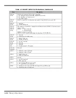
Page 72: ...450 MIDI baud rate support Infrared support on UART2 IrDA 1 0 SIR IrDA 1 1 MIR and FIR and Sharp SIR Address Decoder 6 bit or 10 bit decoding External Chip Select capability when 10 bit decoding Full relocation capability no limitation Enhanced Power Management Special configuration registers for power down Enhanced programmable power down FDC command Auto power down and wake up modes 2 special pi...

Page 73: ...e hard disk drives are factory formatted as a single drive Drive C and are preloaded with installation versions of Windows 95 or Windows for Workgroups in dual load versions the user selects operating system during software installation The Hard Disk Controller is implemented with the PCIO643 Controller Chip described in greater detail in the following paragraph 4 2 8 1 PCI0643 Features Capable of...

Page 74: ...he previous paragraphs 4 2 10 PCMCIA Subsystem The notebook is equipped with a PCMCIA subsystem that accomodates either two Type I or Type II PCMCIA cards or one Type III card The heart of the PCMCIA Subsystem is the TI PCI 1130 high performance PCI to PC Card controller that supports two independent PC Card sockets compliant with the 1995 PC card standard The PCI 1130 provides a set of features t...

Page 75: ...compliant Low Power advanced submicron CMOS technology Uses serial interface to Texas Instruments TI tps2202a dual power switch System interrupts can be programmed as PCI Style or ISA IRQ Style interrupts ISA IRQ interrupts can be serialized onto a single IRQSER pin Independent read and write buffers for each direction Supports burst transfers to maximize data throughput on the PCI and CardBus bus...

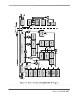
Page 76: ... equipped with a software hardware monitored controlled Power Subsystem that minimizes battery usage for prolonged battery operation and automatically recharges the batteries when the notebook is used with an AC adapter The control for the power subsystem is implemented with the ALI M6377 Power Management Unit chip as described below A simplified block diagram of the power subsystem is shown in Fi...

Page 77: ...PCI1130 SW SW M 1521 M 1523 9088MAL CPU 3 3V SW M 5V SW 2 9V M 2 9V SW M 7V AUDIO_VDD ES1878S SW FLASH ROM 12V M 12V 3 3V 5V 3 3V 5V 5V VGA_VDD M 5V M 3 3V M 5V M 5V L2 CACHE HDD PCI0643 87338 5V M 6375 M 38813 65550 S3 VRAM RESUME GLUE LOGIC M 5V M AX213 SW PCI0643 3 3V 12V 5V SW AD BAT AD BAT SW LCD CD DC2 CD_5V Notebook MPB CHARGER ADVANCED PCI CARD ...

Page 78: ... operation state each pin is programmable and power configurable Provide system activity monitoring including Video Hard disk drive Floppy disk drive Serial port Keyboard Parallel port Two programmable I O groups activity monitor each group contains 16 8 I O addresses One predefined I O group activity monitor Multiple external wake up events from DOZE and SLEEP states External push button RTC alar...

Page 79: ...ccessible 0 MPB s SMBUS is accessible GPIO25 W R 1 Brightness level is fixed 0 Brightness is trimable via GPIO22 GPIO20 The current brightness level is stored when PIO25 low to high transations GPIO24 W R For DSTN LCD only 1 Contrast level is fixed 0 Contrast is trimable via GPIO22 GPIO20 The current brightness level is stored when PIO25 low to high transations GPIO23 1 Normally 0 Ready to transat...

Page 80: ... GPIO35 1 Enable DS1620 0 Disable DS1620 GPIO34 is CLK for 3 wire BUS GPIO33 is DATA must be valid during the rising edge of CLK GPIO34 GPIO32 W R 1 Normally 0 System into STANDBY mode GPIO31 W R 1 Enable 1394 power 0 Disable 1394 power GPIO30 W R 1 Go to 5V suspend 0 Normally SE12 W 1 Normally 0 Disable notebook s OP amplify SE11 W SE10 W Reserved GPIO7 1 Media bay switch is unlocked 0 Media bay ...

Page 81: ...harge the batteries The specifications for the AC adapter include Input Voltage 100 to 250 VAC Input Current Approximately 1 5 Amps Input Frequency 50 to 60 Hz 4 2 12 Mobile Productivity Base Interface Figure 4 5 MPB Interface Diagram PCI0643 SW SW HDD CD MO FDD SW M1521 M1523 PCI1130 PCI0643 PCI PCI 87338 DPCIRST SW 65550 S3 ZV ZV CLOCK GEN M6377 RDATA WDATA IDE PCICLK1 PCICLK2 Advanced PCI Card ...

Page 82: ......

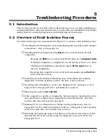
Page 83: ...ss adjustment press Fn Up Arrow keys to increase brightness Ensuring that computer is not set for external monitor press Fn F12 to select internal screen Undocking from the Mobile Productivity Base if installed and running diagnostics to isolate problem to either the base or the notebook Recording and attempting to resolve any displayed error messages or error beeps refer to Paragraph 5 3 3 1 and ...

Page 84: ...AGNOSTICS DIAGNOSTICS ERRORMSG NO YES NO YES See Paragraph 5 3 5 NO YES See Paragraphs 5 3 3 1 and 5 3 3 2 NO See Paragraphs 5 3 1 5 3 2 NO YES See Paragraph 5 5 When Power button is pressed no indication of power is present dark LCD no Status icons lit no disk drive activity etc Press Power button Selftest automatically runs when power turned on MPB TROUBLE INDICATION NO See Paragraph 5 4 ...

Page 85: ...problem check the following AC adapter and Battery Plug in the AC adapter and double check all connections on the adapter and computer Ensure that the Notebook Power switch is set to the On position and that the system is not in Suspend or Sleep mode Measure the voltage at the AC outlet or plug in a known good appliance e g a lamp to verify that voltage is present If the voltage is okay try replac...

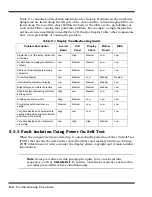
Page 86: ...e you to use keystroke sequences such as Ctrl Alt Del To execute a keystroke sequence such as this you must press all three keys simultaneously Table 5 1 Display Troubleshooting Guide Problem Description Inverter Board LCD Panel Display Cable Mother Board BIOS Single line on LCD display horizontal or vertical Low High Medium Low Low Multiple lines on display horizontal or vertical Low Medium Mediu...

Page 87: ...d other built in utilities If POST fails to complete successfully the display shows one of the error messages described in Table 5 2 Note In the event of a hardware problem that affects the display the Notebook also communicates errors via a series of beeps The interpretation of the beep codes is provided in Table 5 3 Note Refer to Appendix C for POST BIOS listing ...

Page 88: ...k the keyboard controller and system board Turn the power off then back on again If the problem persists contact qualified service personnel Fixed disk configuration error The specified configuration is not supported or doesn t match the actual hardware installed Correct the fixed diskette configuration Fixed disk controller failure The fixed diskette may be defective Try rebooting If that doesn t...

Page 89: ...n the power off then back on again If the problem persists contact qualified service personnel Shutdown failure Either the keyboard controller is not accepting the reset command or the associated reset logic has failed Check the keyboard controller and system board Turn the power off then back on again If the problempersists contact qualified service personnel Time of day not set run SETUP program...

Page 90: ...ontact qualified service personnel Keyboard data line failure The keyboard controller firmware has failed Check the keyboard controller and system board Turn the power off then back on again If the problem persists contact qualified service personnel Keyboard stuck key failure A key is jammed Locate the jammed key and fix it Make sure the keyboard cable and keyboard are connected properly Turn the...

Page 91: ...he event of a hardware software error that occurs after completion of POST the error messages listed and described in Table 5 4 may occur Table 5 3 Self Test Beep Messages Beep Code Description VGA Failures 1 Long 2 Short Horizontal Retrace Failed 1 Long 3 Short DAC Test Failed 1 Long 4 Short Monitor Sense Failed 1 Long Five Short Vertical Retrace Failed 1 Long 6 Short DVideo Memory Test Failed Sy...

Page 92: ... and troubleshoot the notebook using PC Doctor Diagnostics Message Cause Action I O card parity interrupt at address Type S hut off NMI R eboot other keys to continue Memory on a peripheral card has failed Check the memory cards installed in the system Memory parity interrupt at address Type S hut off NMI R eboot other keys to continue A memory chip s has failed Check the memory on the system boar...

Page 93: ...he battery pack is of the right type charged and is inserted correctly 3 Check the powerboard of the system Is it inserted into the motherboard connector properly Otherwise replace the powerboard Data on the LCD is unreadable 1 Adjust the brightness and contrast display controls 2 Check if the LCD cables are inserted properly Check connections inside the LCD panel 3 Verify if installed VGA driver ...

Page 94: ...for 1 5 hours before using again 3 Replace the battery pack System halts during boot sequence 1 Check condition of selected bootload device disk or hard disk for bad boot track or incorrect OS files 2 Try booting from a new bootable disk and recopy or repartition hard disk drive 3 Check for any BIOS error messages on the display screen 4 Replace motherboard I O processing malfunctions 1 Check the ...

Page 95: ...heck if the PCMCIA card is inserted properly and all connections are set 3 Replace the PCMCIA card 4 Replace the motherboard Mouse doesn t work 1 Check if PS 2 mouse driver is properly installed 2 Check the keyboard controller chip for any cold or loosed soldering 3 Replace the motherboard Serial device does not work 1 Check if serial driver is correctly configured 2 Check if serial device is conn...

Page 96: ... COM and LPT ports are assigned and what ports are available identifying partitioning data for fixed disk drive s determining the VGA setup information reading the software interrupts interrupt vectors etc Functionally PC Doctor includes the following Group of non Interactive diagnostic tests that perform a non destructive test of the major hardware functions in the notebook Processor Memory Syste...

Page 97: ...er Enter Key Selects the highlighted option Esc Key Cancels current function and goes back one step F1 Key Activates the context sensitive help feature pressing F1 twice in a row calls up the online Technical Reference Manual for PC Doctor Scrolling windows which show the results of various operations use the following keys Page Up Page Down Moves the screen one page at a time F2 Prints the log to...

Page 98: ......

Page 99: ...tive maintenance is limited to cleaning the plastic case keyboard and the display screen 6 2 1 Cleaning the Computer When it is necessary to clean the plastic case and keyboard use a soft lint free cloth slightly dampened with a mild detergent solution or use the contents of any commercially available computer cleaning kit Caution Never spray any liquids directly on the computer case keyboard or s...

Page 100: ...ields such as those generated by transformers speakers or telephone handsets 6 2 3 Handling the Computer Battery Pack The battery pack furnished with the computer requires reasonable care and handling to ensure efficient operation and maximum life Periodically inspect the battery terminals and the batteries for evidence of corrosion and oxide build up clean if necessary To ensure that the battery ...

Page 101: ...ll flat blade screwdriver Small Phillips screwdriver 5 mm Nut Driver Caution All boards options and peripherals contain components that are sensitive to static electricity When handling any of these items protect against static electricity by using wrist grounding straps and grounded working mats When moving or storing items use the anti static bags supplied with the items 6 4 Notebook FRUs Table ...

Page 102: ...Assembly The Cover Display Assembly shown in Figure 6 2 contains the LCD screen DC AC Inverter Board DC DC Inverter Board bezel LCD cover and various other components as listed in Table 6 1 Mobile Productivity Base Assembly Notebook Assemblies Cover Display Assembly Base Assembly ...

Page 103: ... 5 18 9813637 0001 DISPLAY ASSY DSTN 12 1 SHARP EXT 90X 6 5 7 9813638 0001 CABLE DISPLAY DSTN FJ EXT 90X 6 5 7 9813678 0001 PWB INVERTER TFT EXT 90X 6 5 19 9813639 0001 BEZEL DISPLAY TFT FJ EXT 90X 6 5 17 9813640 0001 LCD PANEL TFT 11 3 FJ EXT 90X 6 5 18 9813641 0001 DISPLAY ASSY TFT 11 3 SHARP EXT 90X 6 5 7 9813642 0001 CABLE INVERTER WIRE 12P EXT 900 6 5 19 9813680 0001 CN2 Latch Securing Invert...

Page 104: ...ence paragraph numbers containing removal replacement procedures are listed in Table 6 2 Figure 6 3 Notebook Base Assembly Major FRUs Power Supply Board Battery Connector Cable Assembly Main Board CPU Board Touchpad Assembly TOP Cover VGA Video Board PC Card Module LED Board Battery Keyboard Assembly Microphone LCD Speaker Speaker Notebook with Keyboard and Battery Removed Heatsink Assembly ...

Page 105: ...1 KEYBOARD UK EXT 900 6 5 5 9813648 0002 KEYBOARD GER EXT 900 6 5 5 9813648 0003 KEYBOARD FRA EXT 900 6 5 5 9813648 0004 KEYBOARD SPA EXT 900 6 5 5 9813648 0005 KEYBOARD SWI GER FRA EXT 900 6 5 5 9813648 0006 KEYBOARD ITA EXT 900 6 5 5 9813648 0007 KEYBOARD POR EXT 900 6 5 5 9813648 0008 KEYBOARDS SWE EXT 900 6 5 5 9813648 0010 KEYBOARD DEN EXT 900 6 5 5 9813648 0012 KEYBOARD NOR EXT 900 6 5 5 981...

Page 106: ...WP 0 2 2 0 17 Ref 9813665 0001 HINGE RIGHT EXT 900 Ref 9813666 0001 HINGE LEFT EXT 900 Ref 9813667 0001 KNOB BATTERY EXT 900 Ref 9813668 0001 COVER HDD EXT 900 Ref 9813669 0001 TUBE FOR LCD ABS 072 EXT 900 Ref 9813674 0001 BATTERY LOCK RIGHT EXT 900 Ref 9813675 0001 BATTERY LOCK LEFT EXT 900 Ref 9813676 0001 DOOR SLIDE PC FB 082 EXT 900 Ref 9813677 0001 ASSY CORE UPPER CASE EXT 900 Ref 9813681 000...

Page 107: ... Ref 9813658 0001 PWB ASSY MAIN BOARD MPB EXT 90X 6 6 7 9813661 0001 PWB ASSY DC IN BOARD MPB EXT 90X 6 6 6 9813662 0001 PWB ASSY BATTERY BOARD EXT 900 same as used in Notebook Ref 9813656 0001 CASE UPPER MPB EXT 90X Ref 9813659 0001 CABLE ASSY DOC MPB EXT 90X Ref 9813660 0001 KNOB HAND LEVER LOCK MPB EXT 900 Ref 9813670 0001 KNOB MODULE LATCH MPB EXT 900 Ref 9813671 0001 LOCK HAND LEVER MPB EXT 9...

Page 108: ...U removal replacement procedures involve connecting and disconnecting cable connectors The Extensa series uses two types of connectors including Locking type connectors Use a plastic stick to unlock and lock these type of connectors as shown in Figure 6 5 Non locking connectors MPB with Upper Cover Removed DC DC Converter Dock Mechanism Main Board Assembly Lever Release Latch Dock Release Lever Up...

Page 109: ...ook and remove all battery packs The procedure for removing and replacing the notebook battery pack is as follows 1 Turn off the computer and disconnect the AC adapter from the computer 2 Unlock the battery on each side of the notebook and pull the battery out of the front of the notebook as shown in Figure 6 6 3 Replacement is essentially the reverse of Steps 1 and 2 connector side of battery goe...

Page 110: ...Paragraph 6 5 1 2 Press the upper card eject button to eject the upper card lower button controls the lower card and use both buttons for Type III devices 3 To replace the PCMCIA device remove any filler cards present and insert the device Reinstall any external cabling required for the device Unlock the Battery Pull Battery Out of Unit Unlock Battery Pack Remove Battery from Front of Notebook If ...

Page 111: ...re for removing and replacing the Mobile Productivity Base assembly is as follows 1 Power down the notebook and disconnect the AC adapter if installed 2 Slide the lever release latch to the front of the MPB to release the docking lever refer to Figure 6 8 3 Swing the Docking Lever outward a full 90 degrees from the side of the MPB ...

Page 112: ...e MPB left side first as shown in Figure 6 8 6 Close the lever and close the expansion door on the bottom of the computer 7 To replace the notebook in the MPB turn the notebook over and open the expansion door slide the door toward the center of the notebook 8 Slide the Release latch toward the front of the MPB to release the lever then swing the lever completely away from the MPB until the lever ...

Page 113: ...isk Drive Assembly The procedure for removing and replacing the Hard Disk Drive assembly is as follows 1 Power down the notebook disconnect the AC adapter if installed and remove the battery pack as described in Paragraphs 6 5 1 and 6 5 2 2 Disconnect the Mobile Productivity Base and any installed PCMCIA options 3 Turn the computer over and remove the hard disk drive bay cover refer to Figure 6 9 ...

Page 114: ...ed in Paragraphs 6 5 1 and 6 5 2 Also disconnect the MPB Paragraph 6 5 3 if attached 2 Remove the four screws near the display hinges rear of the notebook as shown in Figure 6 10 3 Snap out and pull up the Status Panel refer to Figure 6 10 Figure 6 10 Removing the Keyboard Assembly 4 Lift up the Keyboard Assembly to free it from the notebook and then flip the keyboard to the left side of the noteb...

Page 115: ...wer adapter if it is attached and remove the battery pack and PCMCIA cards as described in Paragraphs 6 5 1 and 6 5 2 Also disconnect the MPB Paragraph 6 5 3 if attached 2 Remove the Keyboard Assembly as described in Paragraph 6 5 5 3 Remove the four screws securing the Heat Sink Assembly to the notebook and remove the heat sink 4 Replacement of the Heat Sink Assembly is the reverse of Steps 1 thr...

Page 116: ...raph 6 5 5 3 Remove the Heat Sink Assembly as described in Paragraph 6 5 6 4 Refer to Figure 6 12 and remove the two rear screws that secure the Display to the notebook housing Note You don t have to remove the leftmost screw Figure 6 12 Removing Replacing the Display Assembly 5 Remove the screw securing the Display Cable to the Main Board and unplug the Display Cable CN1 and the Inverter Cable CN...

Page 117: ...MPB Paragraph 6 5 3 if attached 2 Remove the Keyboard Assembly as described in Paragraph 6 5 5 3 Remove the Heat Sink Assembly as described in Paragraph 6 5 6 4 Remove the Display Assembly as described in Paragraph 6 5 7 5 Remove the two screws that secure the LED Board Assembly and unplug cable connector CN7 remove the LED Board Assembly 6 Replacement is the reverse of Steps 1 through 5 Figure 6 ...

Page 118: ...nd 6 5 2 Also disconnect the MPB Paragraph 6 5 3 if attached 2 Remove the Keyboard Assembly as described in Paragraph 6 5 5 3 Remove the Heat Sink Assembly as described in Paragraph 6 5 6 4 Remove the screw securing the CPU Board to the Main Board and pull up to remove the board from connector J1 5 Replacement is the reverse of Steps 1 through 4 Figure 6 14 CPU Board Assembly Removal Replacement J...

Page 119: ... attached 2 Remove the Keyboard Assembly as described in Paragraph 6 5 5 3 Remove the Heat Sink Assembly as described in Paragraph 6 5 6 4 Remove the Display Assembly as described in Paragraph 6 5 7 5 Remove four screws from the bottom of the base assembly 6 Turn the base assembly over and remove Touchpad Speaker connector CN19 7 Remove four screws from the four corners of the top cover Figure 6 1...

Page 120: ...ing Replacing the Top Cover 3 Unplug Speaker Connector CN19 an remove screws at fo corners 1 2 Remove keyboard and Heat Sink Assemblies Remove four Screws at Bottom of Main Unit 4 Beginning at left side unsnap top cover from base assembly ...

Page 121: ...Paragraph 6 5 3 if attached 2 Remove the Keyboard Assembly as described in Paragraph 6 5 5 3 Remove the Heat Sink Assembly as described in Paragraph 6 5 6 4 Remove the Display Assembly as described in Paragraph 6 5 7 5 Remove two screws and unplug the VGA Video Board from the Main Board as shown in Figure 6 16 6 Replacement is the reverse of Steps 1 through 5 Figure 6 16 Removing Replacing the VGA...

Page 122: ... 5 1 and 6 5 2 Also disconnect the MPB Paragraph 6 5 3 if attached 2 Remove the Keyboard Assembly as described in Paragraph 6 5 5 3 Remove the Heat Sink Assembly as described in Paragraph 6 5 6 4 Remove the screw that secures the Power Supply Board Assembly to the Main Board and remove the board from the base assembly 5 Replacement is the reverse of Steps 1 through 4 Figure 6 17 Removing Replacing...

Page 123: ...attery pack and PCMCIA cards as described in Paragraphs 6 5 1 and 6 5 2 Also disconnect the MPB Paragraph 6 5 3 if attached 2 Remove the Keyboard Assembly as described in Paragraph 6 5 5 3 Remove the Heat Sink Assembly as described in Paragraph 6 5 6 4 Unplug cable connectors CN9 and CN10 and remove the board 5 Replacement is the reverse of Steps 1 through 4 Figure 6 18 Removing Replacing the DC I...

Page 124: ...phs 6 5 1 and 6 5 2 Also disconnect the MPB Paragraph 6 5 3 if attached 2 Remove the Keyboard Assembly as described in Paragraph 6 5 5 3 Remove the Heat Sink Assembly as described in Paragraph 6 5 6 4 Remove the Display Assembly as described in Paragraph 6 5 7 5 Remove the four screws that secure the PC Card Module to the Main Board refer to Figure 6 19 6 Replacement is the reverse of Steps 1 thro...

Page 125: ...attached 2 Remove the Keyboard Assembly as described in Paragraph 6 5 5 3 Remove the Heat Sink Assembly as described in Paragraph 6 5 6 4 Remove the Display Assembly as described in Paragraph 6 5 7 5 Remove the Top Cover Assembly as described in Paragraph 6 5 10 6 Remove fourteen screws from the bottom assembly as shown in Figure 6 20 7 Remove the top cover as described in Paragraph 6 5 10 8 Remov...

Page 126: ...graph 6 5 5 3 Remove the Heat Sink Assembly as described in Paragraph 6 5 6 4 Remove the Display Assembly as described in Paragraph 6 5 7 5 Remove the Top Cover Assembly as described in Paragraph 6 5 10 6 Remove the connectors on both sides of the Touchpad Assembly and detach speakers from the top cover 7 Remove the two screws that secure the Touchpad Assembly to the Top Cover and remove the Butto...

Page 127: ... adapter if it is attached and remove the battery pack and PCMCIA cards as described in Paragraphs 6 5 1 and 6 5 2 Also disconnect the MPB Paragraph 6 5 3 if attached 2 Use a sharp object to remove the six bezel screw covers and remove the six screws 3 Pull out and remove the Display Bezel 4 Replacement is the reverse of Steps 1 through 3 Figure 6 22 Removing Replacing the Display Bezel ...

Page 128: ... 6 5 1 and 6 5 2 Also disconnect the MPB Paragraph 6 5 3 if attached 2 Remove the Display Bezel as described in Paragraph 6 5 17 3 Remove three screws securing the LCD Assembly and pull up on the LCD Panel Figure 6 23 4 Tilt the LCD Panel away from the display cover unplug the LCD Panel from the Display Cable Assembly Figure 6 23 and remove the LCD Assembly 5 Replacement is the reverse of Steps 1 ...

Page 129: ...connect the MPB Paragraph 6 5 3 if attached 2 Remove the Display Bezel as described in Paragraph 6 5 17 3 Gently fold back the foil around the display and unplug the inverter cable CN2 4 Next remove the screw securing the DC AC Inverter Board larger of the two PWBs and the LCD ID Board smaller of the PWBs to the display back cover 5 Press down on the latch refer to Figure 6 24 and remove the Inver...

Page 130: ...attery pack and PCMCIA cards as described in Paragraphs 6 5 1 and 6 5 2 Also disconnect the MPB Paragraph 6 5 3 if attached 2 Unlatch the module by pressing the latch at the base of the MPB toward the unlock icon rear of MPB refer to Figure 6 25 3 Simultaneously grasp the recessed grip area on the module and pull module out of the MPB 4 Installation is the reverse of Steps 1 through 3 Figure 6 25 ...

Page 131: ...and remove the battery pack and PCMCIA cards as described in Paragraphs 6 5 1 and 6 5 2 Also disconnect the MPB Paragraph 6 5 3 if attached 2 Using your thumbs unlock the two battery locks at each side of the MPB refer to Figure 6 26 3 Pull the module out of the MPB 4 Installation is the reverse of Steps 1 through 3 Figure 6 26 Installing Removing Battery Pack in MPB Unlocking the Battery Battery ...

Page 132: ...3 Pull the module out of the MPB 4 Slide the Lever Release Latch forward to release the Docking Lever extend Docking Lever 90 degrees from the side of the MPB 5 Remove fourteen screws from the top of the MPB as shown in Figure 6 27 6 Lift up on the top section of the MPB Housing from the left side as shown in Figure 6 27 then pull to remove the top section of the MPB 7 Replacement is the reverse o...

Page 133: ...ng your thumbs unlock the two battery locks at each side of the MPB refer to Figure 6 26 pull the battery pack out of the MPB 3 Remove the MPB Housing as described in Paragraph 6 6 3 4 Remove two screws securing the Docking Cable to release the assembly refer to Figure 6 28 5 Remove the four screws securing the Docking Cable assembly to the Docking Mechanism and remove the Docking Cable 6 Replacem...

Page 134: ...PB Paragraph 6 5 3 if attached 2 Using your thumbs unlock the two battery locks at each side of the MPB refer to Figure 6 26 pull the battery pack out of the MPB 3 Remove the MPB Housing as described in Paragraph 6 6 3 4 Remove the Docking Cable as described in Paragraph 6 6 4 5 Remove the two screws that secure the Docking Mechanism to the bottom section of the housing and remove the Docking Mech...

Page 135: ...d 6 5 2 Also disconnect the MPB Paragraph 6 5 3 if attached 2 Using your thumbs unlock the two battery locks at each side of the MPB refer to Figure 6 26 pull the battery pack out of the MPB 3 Remove the MPB Housing as described in Paragraph 6 6 3 4 Remove the screw that secures the DC DC Converter to the bottom section of the MPB housing and remove the DC DC Converter 5 Replacement is the reverse...

Page 136: ...attery pack out of the MPB 3 Remove the MPB Housing as described in Paragraph 6 6 3 4 Remove the MPB Docking Cable and Docking Mechanism as described in Paragraphs 6 6 4 and 6 6 5 5 Remove the screw that secures the DC DC Converter to the bottom section of the MPB housing and remove the DC DC Converter 6 Remove the DC In and Battery Charger Cable Connectors CN 13 and CN10 7 Remove the 12 screws th...

Page 137: ... A 1 A Notebook Schematic Diagrams A 1 Introduction This section contains schematic diagrams for the Extensa 900 Series Notebook Computer Logic schematics for the Mobile Productivity Base are provided in Appendix B of this manual ...

Page 138: ...A 2 Notebook Schematic Diagrams Figure A 1 Notebook Main Board Logic Diagrams Sheet 1 of 30 ...

Page 139: ...Notebook Schematic Diagrams A 3 Figure A 1 Notebook Main Board Logic Diagrams Sheet 2 of 30 ...

Page 140: ...A 4 Notebook Schematic Diagrams Figure A 1 Notebook Main Board Logic Diagrams Sheet 3 of 30 ...

Page 141: ...Notebook Schematic Diagrams A 5 Figure A 1 Notebook Main Board Logic Diagrams Sheet 4 of 30 ...

Page 142: ...A 6 Notebook Schematic Diagrams Figure A 1 Notebook Main Board Logic Diagrams Sheet 5 of 30 ...

Page 143: ...Notebook Schematic Diagrams A 7 Figure A 1 Notebook Main Board Logic Diagrams Sheet 6 of 30 ...

Page 144: ... 134 136 138 140 142 144 143 146 145 CN12 SDIMM144 MA 0 11 MD 0 63 MD0 MD1 MD2 MD3 MD4 MD5 MD6 MD7 CAS 0 CAS 1 MD 0 63 DRAM_VCC DIMM SOCKET 2 6 2 2 2 RAS 2 RAS 3 MWE MD8 MD9 MD10 MD11 MD12 MD13 MD14 MD15 MA0 MA1 MA2 9 1 2 R202 100KR3 DIMM_IN MD40 MD41 MD42 MD43 MD44 MD45 MD46 MD47 MA3 MA4 MA5 M 5V 23 19 MOS_ON ID_CLK 9 8 1 4 1 0 7 U51C SOLCX125M 1 2 R154 100KR3 MD48 MD49 MD50 MD51 MD52 MD53 MD54 M...

Page 145: ...Notebook Schematic Diagrams A 9 Figure A 1 Notebook Main Board Logic Diagrams Sheet 8 of 30 ...

Page 146: ...A 10 Notebook Schematic Diagrams Figure A 1 Notebook Main Board Logic Diagrams Sheet 9 of 30 ...

Page 147: ...Notebook Schematic Diagrams A 11 Figure A 1 Notebook Main Board Logic Diagrams Sheet 10 of 30 ...

Page 148: ...A 12 Notebook Schematic Diagrams Figure A 1 Motherboard PWB Logic Diagrams Sheet 11 of 23 ...

Page 149: ...Notebook Schematic Diagrams A 13 Figure A 1 Notebook Main Board Logic Diagrams Sheet 12 of 30 ...

Page 150: ... RTC SB ADD DUMMY RESISTER TO 14 ENEXTCMOS 4 SA 0 15 A0 12 A1 11 A2 10 A3 9 A4 8 A5 7 A6 6 A7 5 A8 27 A9 26 A10 23 A11 25 A12 4 A13 28 A14 29 A15 3 A16 2 CE 22 VCC 32 VSS 16 VPP 1 DQ0 13 DQ1 14 DQ2 15 DQ3 17 DQ4 18 DQ5 19 DQ6 20 DQ7 21 PGM 31 OE 24 A17 N C 30 U45 S128K8 150 SA0 SA1 5V BIOS ROM C213 SCD1U 1 2 3 4 5 6 D16 RB731U SB ADD 100KR3 FOR QUICK DISCHARGE 4 3 2 1 Q6 S2N3906 1 2 R147 10KR3 C22...

Page 151: ... 4 13 15 17 19 20 25 C153 SCD1U 1 2 L12 SCHOKE D C154 SC1KP SD 0 7 KROW6 KROW7 KROW8 SD 0 7 KBC_5V M 5V 4 4 4 20 26 26 13 IOW IOR SA2 KBCS TDATA TCLK ENEXTCMOS SD3 SD4 SD5 SD6 SD7 SD0 SD1 SD2 KROW1 KROW2 KROW3 KROW4 KROW5 SA2 IOR IOW TDATA TCLK KBCS 1 2 RX09 20KR3 CLLED NLLED CLLED NLLED IRQ1 IRQ12 B_SMB_DATA B_SMB_CLK KBCLK KBDATA 5V M38813 SB ADD 20K PULL UP TO SUSRST SB ADD IRQ1 PULL UP 4 4 10 ...

Page 152: ...15 67 RI1 68 DTR1 69 CTS1 70 SOUT1 BOUT1 BADDR1 71 RTS1 BADDR0 72 SIN1 73 DSR1 74 DCD1 75 A F D D S T R B D E N S E L 7 6 E R R H D S E L 7 7 I N I T D I R 7 8 S L I N S T E P A S T R B 7 9 S L C T W G A T E 8 0 P E W D A T A 8 1 B U S Y W A I T M T R 1 8 2 A C K D R 1 8 3 P D 7 M S E N 1 8 4 P D 6 D R A T E 0 8 5 P D 5 M S E N 0 8 6 P D 4 D S K C H G 8 7 V S S 8 8 P D 3 R D A T A 8 9 P D 2 W P 9 ...

Page 153: ...Notebook Schematic Diagrams A 17 Figure A 1 Notebook Main Board Logic Diagrams Sheet 16 of 30 ...

Page 154: ...A 18 Notebook Schematic Diagrams Figure A 1 Notebook Main Board Logic Diagrams Sheet 17 of 30 ...

Page 155: ...Notebook Schematic Diagrams A 19 Figure A 1 Notebook Main Board Logic Diagrams Sheet 18 of 30 ...

Page 156: ...A 20 Notebook Schematic Diagrams Figure A 1 Notebook Main Board Logic Diagrams Sheet 19 of 30 ...

Page 157: ...Notebook Schematic Diagrams A 21 Figure A 1 Notebook Main Board Logic Diagrams Sheet 20 of 30 ...

Page 158: ...A 22 Notebook Schematic Diagrams Figure A 1 Notebook Main Board Logic Diagrams Sheet 21 of 30 ...

Page 159: ...Notebook Schematic Diagrams A 23 Figure A 1 Notebook Main Board Logic Diagrams Sheet 22 of 30 ...

Page 160: ...A 24 Notebook Schematic Diagrams Figure A 1 Notebook Main Board Logic Diagrams Sheet 23 of 30 ...

Page 161: ...Notebook Schematic Diagrams A 25 Figure A 1 Notebook Main Board Logic Diagrams Sheet 24 of 30 ...

Page 162: ...31 B32 32 B33 33 B34 34 B35 35 B36 36 B37 37 B38 38 B39 39 B40 40 A1 41 A2 42 A3 43 A4 44 A5 45 A6 46 A7 47 A8 48 A9 49 A10 50 A11 51 A12 52 A13 53 A14 54 A15 55 A16 56 A17 57 A18 58 A19 59 A20 60 A21 61 A22 62 A23 63 A24 64 A25 65 A26 66 A27 67 A28 68 A29 69 A30 70 A31 71 A32 72 A33 73 A34 74 A35 75 A36 76 A37 77 A38 78 A39 79 A40 80 GF1 MS DBG GF80 SD 0 15 5V DEBUG BD GOLDEN FINGER 4 4 4 4 4 4 4...

Page 163: ...BCLK KBDATA C79 SC47P 1 2 R1 47R3 1 2 R2 47R3 1 2 R4 47R3 1 2 R3 47R3 1 2 L4 MLB321611 1 2 L5 MLB321611 1 2 L7 MLB321611 1 2 L6 MLB321611 1 2 3 4 5 6 7 8 CN9 SD5339810 6 C78 SC47P C77 SC47P C76 SC47P 14 TDATA 18 18 14 1 3 5 7 9 11 13 2 4 6 8 10 12 14 15 16 17 18 CN19 SD5255917 14 1 2 3 4 5 6 7 8 RP31 SRN10K SPK_L1 SPK_R1 TCLK 5V 5V TOUCHPAD CONNECTOR SB CHANGE CN19 PIN DEFINITION C234 SC47P C224 S...

Page 164: ...5VSB BAT BAT CSI CSO CHARGER HANDSHAKING SIGNALS 19 21 2 1 D28 NSQ03A04 1 DCBATOUT ADAPTOR BATTERY INTERFACE AD 1 2 R242 560R3 1 2 3 D22 BAV99 DK_ADBATON BL3 DCBATOUT 1 2 3 4 8 7 6 5 U94 SI4435DY 2 1 D27 NSQ03A04 1 1 2 3 Q13 2N7002 1 2 RY16 4K7R3 2 1 DY6 MBR0540T1 1 2 R270 240KR3 1 2 R269 100KR3 1 3 DY1 BZX84C4V3L BAT CY13 SCD1U50V3ZY 330KR3 82KR3 1 2 RY23 220KR3 1 2 3 QY1 2N7002 2 2KR3 CY14 SCD1U...

Page 165: ...E_LED NLOCK_LED CLOCK_LED M 5V 5VSB SB ADD LOWBAT_LED 19 29 1 3 5 7 9 11 13 2 4 6 8 10 12 14 15 17 19 16 18 20 CN7 SD5255917 16 POWER_SW2 LOWBAT_LED POWER_SW2 STANDBY_LED HDD FDD_LED 5V MIC_R AUD_GND 18 INTMIC 19 21 24 1 2 R141 10KR3 HDD_LED DK_DISKLED HDD FDD_LED 5V CLOSE TO CONNECTOR CLOSE TO AUDIO CHIP 19 C59 SC1U10V5JY 9 8 1 4 7 U8D SSHC14 12 11 1 4 1 3 7 U56D SSHC125 STNDBY STANDBY_LED 5V 5V ...

Page 166: ...A 30 Notebook Schematic Diagrams Figure A 1 Notebook Main Board Logic Diagrams Sheet 29 of 30 ...

Page 167: ... 4 7 U67C SSHC32 4 5 6 1 4 7 U67B SSHC32 1 2 3 1 4 7 U54A SSHC08 9 10 8 1 4 7 U91C SSHC08 M 5V M 5V 5V 5VSB 12 13 11 1 4 7 U67D SSHC32 1 2 3 1 4 7 U14A TSHCT00 D 2 CLK 3 Q 5 Q 6 VCC 14 P R 4 GND 7 C L 1 U64A SSHCT74 M 5V 5V 12 13 11 1 4 7 U91D SSHC08 5VSB 5V M 3 3V 8 9 1 4 7 6 U75D SOHC4066 M 3 3V M 3 3V M 3 3V AUDIO_ 5VA AUD_GND D 12 CLK 11 Q 9 Q 8 VCC 14 P R 1 0 GND 7 C L 1 3 U43B SSHC74 12 13 1...

Page 168: ......

Page 169: ...c Diagrams B 1 B MPB Schematic Diagrams B 1 Introduction This section contains schematic diagrams for the Extensa 900 Mobile Productivity Base Logic schematics for the MPB are provided in Appendix A of this manual ...

Page 170: ...LDA WB WT 2 2 2 2 2 2 2 2 2 2 2 2 2 2 CPUCLK CPUINIT CPURST SMI STPCLK BE 7 BE 6 BE 5 BE 4 BE 3 BE 2 BE 1 BE 0 2 2 3 2 3 2 2 CPU_A 3 31 BE 0 7 2 2 C38 SC22U10V0JY 1 3 2 NF1 STC222B VCC_3V C32 SC1KP C14 SC1KP C3 SC22U10V0JY VCC_I O CPU BOARD CONNECTOR LINK CPU1 SCH CPU2 SCH CPU_VCC 101 102 103 104 105 106 107 108 109 110 111 112 113 114 115 116 117 118 119 120 121 122 123 124 125 126 127 128 129 13...

Page 171: ...MPB Schematic Diagrams B 3 Figure B 1 MPB CPU Board Logic Diagrams Sheet 2 of 3 ...

Page 172: ... Not install X X O O X X X1 5 X2 0 X2 5 O O X O O X X O C19 SCD1U C43 SCD1U C4 SCD1U C2 SCD1U VCC_CPU C9 SCD1U C21 SCD1U C16 SCD1U C12 SCD1U C6 SCD1U VCC_CPU C17 SCD1U C28 SCD1U C41 SCD1U C5 SCD1U C23 SCD1U C8 SCD1U C24 SCD1U C10 SCD1U C11 SCD1U C35 SCD1U C39 SCD1U C31 SCD1U C42 SCD1U C52 SCD1U VCC_I O 1 2 R26 10KR3 CPU_THM C47 SCD1U CPU_VEND CPU_ID2 CPU_ID3 FOR SHIVA SHIGA NOT INS 1 2 3 4 5 6 7 8...

Page 173: ... B 2 MPB Battery Board Logic Diagrams Sheet 1 of 1 CLOSE BATTRY CONN PIN1 1 2 3 4 5 6 7 8 CN1 AMP CON8 1 2 3 4 5 6 7 8 CN2 MOLEX CON8 C1 SC1000P50V3MX C2 SC1000P50V3MX C3 SC1000P50V3MX C4 SC1000P50V3MX C5 SC1000P50V3MX C6 SC1000P50V3MX ...

Page 174: ...T_G CRT_R RGB_GND RGB_GND 5 10 5 10 5 10 NOT INSTALL 1 2 R143 10KR3 1 2 R18 47KR3 FRAME PCIRST DEVSEL 5V 1 2 R144 47KR3 1 2 R145 47KR3 1 2 R146 47KR3 TRDY IRDY POWER SCH LINK DOCKIDE SCH FEATURE SCH DOCKPORT SCH CHARGER SCH CD_FDD SCH PAGE 2 PAGE 1 PAGE 3 PAGE 4 PAGE 5 PAGE 6 PAGE 7 PS2_CONN SCH PAGE 8 PAGE 9 AUDIO SCH PAGE 10 TP SCH Docking conn UMA IDE I F PCI0643Q Feature board conn CD HDD FDD ...

Page 175: ...V SC 1 2 RX6 10KR3 SB 1 2 R22 22R3 1 2 R37 4K7R3 1 2 R38 0R3 IRQ15 IDE_IRQ TP269 1 10 3 NOT INSTALL 1 2 3 4 5 6 7 8 RP21 SRN22 C6 SC470P IDE_A0 IDE_A1 IDE_A2 IDE_IOW IDE_IOR IDE_CS0 IDE_CS1 IDE_RST IDE_A0 IDE_A1 IDE_A2 IDE_RST 3 10 3 10 3 10 3 10 3 10 3 10 3 10 3 10 1 2 3 4 5 6 7 8 RP19 SRN22 1 2 3 4 5 6 7 8 RP20 SRN22 1 2 3 4 5 6 7 8 RP22 SRN22 1 2 R31 2K2R3 IDE_D0 IDE_D1 IDE_D2 IDE_D3 IDE_D4 IDE...

Page 176: ...B 8 MPB Schematic Diagrams Figure B 3 MPB Main Board Motherboard Logic Diagrams Sheet 3 of 10 ...

Page 177: ...L 1 2 R159 1KR6 1 2 R162 1KR6 DK_LINEIN_R DK_LINEIN_L DK_PJIN DK_MIC_PJIN LINE_OUT_L LINE_OUT_R DK_PJIN AD AUD_GND 1 1 1 10 1 1 2 C82 ST47U10VDM 1 2 C83 ST47U10VDM 1 2 R99 56KR3 DK_MIC LINE_OUT_L LINE_OUT_R TP333 TP328 AMP_5V AUD_GND 1 IN_A 2 IN_B 6 BYPASS 3 SHUTDOWN 5 OUT_A 1 OUT_B 7 V D D 8 G N D 4 U19 LM4880M 1 2 R97 20KR3 1 2 R98 20KR3 C81 SC1U C84 SCD1U DK_SOUND_L DK_SOUND_R DK_PJIN TP329 TP3...

Page 178: ...B 10 MPB Schematic Diagrams Figure B 3 MPB Main Board Motherboard Logic Diagrams Sheet 5 of 10 ...

Page 179: ... 1 3 10 1 2 R56 100KR3 C22 SCD1U 1 2 D1 S1N4148 3 1 2 Q1 RN1424 13 12 1 4 7 U3F SSHC14 1 2 3 1 4 7 U12A SSHC32 CD_LOCK CD_LOCK TP83 TP296 TP345 5V 5V 5V 1 10 11 10 1 4 7 U3E SSHC14 2 1 3 SW1 DS 1200 02 1 2 R115 100KR3 1 2 R127 10KR3 1 2 1 4 7 U3A SSHC14 1 2 R59 2MR5 1 2 D2 S1N4148 TP308 CD_5V 5V 5V C23 SC1U C96 SCD1U C97 SCD1U C98 SCD1U C99 SCD1U C100 SCD1U 5V BAT C101 SCD1U C102 SCD1U C103 SCD1U ...

Page 180: ... 1 D8 NSQ03A04 1 TP244 DCBATOUT AD 4 3 1 4 7 5 U22C SOHC4066 5VSB 5VSB DK_BL3 LOOPBACK 1 2 RX1 100KR3 5VSB CX3 SCD1U 1 2 3 DX3 BAV99 1 2 RX3 1KR3 SC EN_CHGR_ROM I2C_CLK I2C_DATA 1 1 8 10 1 10 1 2 1 4 7 1 3 U22A SOHC4066 11 10 1 4 7 1 2 U22B SOHC4066 ID_CLK ID_DATA 5VSB 5VSB 1 2 R142 100KR3 1 2 R91 1MR3 DK_BL3 TP327 5V 1 2 R106 0R3 1 2 R107 0R3 1 2 R108 DUMMY R3 5V TP336 TP335 TP337 1 2 R109 DUMMY ...

Page 181: ...ST10U Y1 Y3 Y5 Y7 UV1 UV3 UV5 UV7 ZV_HREF ZV_VREF 1394POWER I2C_CLK ZV_MCLK 1394POWER FLASH_VPP FBCLK Y1 Y3 Y5 Y7 UV1 UV3 UV5 UV7 ZV_HREF 3 3V IIMCLK ZV_VREF 1394 1 1394 3 1394 5 1394 7 1394 9 12V 5V 3 3V 1 7 1 10 1 10 1 10 1 10 1 10 1 10 1 10 1 10 1 10 1 10 1 10 6 2N3906 1 2 R116 10KR3 3 1 2 Q9 RN1424 1 2 R147 10KR3 FLASH_ON TP306 TP342 12V 1 PCI ID INTB REQ 0 C BE 2 SERR PAR DEVSEL IRDY ZV_SCLK ...

Page 182: ...8 CN11 KBMS CONN 1 2 R93 47R3 1 2 R94 47R3 1 2 L3 MLB321611 1 2 F2 SPOLY100 KBCLK KBDATA TP117 TP42 TP41 5V 1 1 10 15V 1 1A SMD100 1 2 R95 47R3 1 2 R96 47R3 1 2 L6 MLB321611 1 2 F3 SPOLY100 PS2DATA PS2CLK TP38 TP40 TP39 5V 1 1 10 15V 1 1A SMD100 KEYBOARD CONN C77 SC47P C78 SC47P 1 2 L4 MLB321611 1 2 L5 MLB321611 6 4 2 1 3 5 7 9 8 CN12 KBMS CONN MOUSE CONN C79 SC47P C80 SC47P 1 2 L8 MLB321611 1 2 F...

Page 183: ...T276 TP 1 T277 TP 1 T278 TP 1 T279 TP 1 T280 TP 1 T281 TP 1 T283 TP 1 T284 TP 1 T287 TP 1 T288 TP 1 T289 TP 1 T290 TP 1 T291 TP 1 T295 TP 1 T187 TP 1 T188 TP 1 T189 TP 1 T190 TP 1 T192 TP 1 T194 TP 1 T196 TP 1 T204 TP 1 T250 TP 1 T251 TP 1 T252 TP 1 T253 TP 1 T254 TP 1 T255 TP 1 T256 TP 1 T258 TP 1 FBDATA IDE_IRQ IDE_IOR IDE_A1 IDE_IOW IDE_CS1 IDE_CS0 C BE 2 IDE_D12 IDE_D13 IDE_D14 IDE_D15 REQ 1 I...

Page 184: ... 0 3 Y 0 7 UV 0 7 ENAVEE AD 0 31 Y 0 7 UV 0 7 C BE 0 3 AD 0 31 C52 SCD1U 2 4 2 2 C10 SCD1U C29 SCD1U ZV_VREF DISPLAY DDC_DATA DDC_CLK C BE 0 ENAVEE ZV_HREF ZV_VREF ZV_PCLK DISPLAY CRT_B AD0 AD1 AD2 AD3 AD4 AD5 AD6 AD7 AD8 AD9 AD10 AD11 AD12 AD13 Y0 Y1 Y2 Y3 Y4 Y5 Y6 Y7 UV0 UV1 UV2 UV3 UV4 5V 2 2 2 4 1 2 R10 47R3 C17 SC39P 1 2 R22 47R3 C40 SC39P ZV_HREF ZV_PCLK CRT_B LCDVEE FRAME 5V C53 SCD1U 1 2 R...

Page 185: ...1 0 1 3 7 M B D 1 1 1 3 8 M B D 1 2 1 4 0 M B D 1 3 1 4 1 M B D 1 4 1 4 3 M B D 1 5 1 4 4 RASB 123 CASBH 125 CASBL 126 WEB 124 P8 81 P9 82 P10 83 P11 84 P12 85 P13 86 P14 87 P15 88 ACTI 53 ENABKL 54 M 69 A20 199 ROMOE 200 CLK 201 A23 28 SERR 30 M V C C B 1 4 2 I V C C 1 8 1 C V C C 0 2 0 5 C V C C 1 2 0 6 C G N D 0 2 0 2 C G N D 1 2 0 8 RSET 55 PERR 29 A D 1 9 1 7 A D 2 0 1 6 A D 2 1 1 5 A D 2 2 1...

Page 186: ...6 9 DQ7 10 N C 11 N C 12 N C 13 N C 14 WE 15 RAS 16 N C 17 A0 18 A1 19 A2 20 A3 21 VCC 22 VSS 44 DQ15 43 DQ14 42 DQ13 41 DQ12 40 VSS 39 DQ11 38 DQ10 37 DQ9 36 DQ8 35 N C 34 N C 33 N C 32 LCAS 31 UCAS 30 OE 29 A8 28 A7 27 A6 26 A5 25 A4 24 VSS 23 U5 S256K16 60 CASBH CASBL VAA4 VAA5 VAA6 VAA7 VAA8 CASBH CASBL OE VMBD8 VMBD9 VMBD10 VMBD11 VMBD12 VMBD13 VMBD14 VMBD15 2 2 C31 SCD1U RASB WEB VAA0 VAA1 V...

Page 187: ...17 18 19 20 21 22 23 24 25 26 27 28 29 30 31 32 33 34 35 36 37 38 39 40 80 79 78 77 76 75 74 73 72 71 70 69 68 67 66 65 64 63 62 61 60 59 58 57 56 55 54 53 52 51 50 49 48 47 46 45 44 43 42 41 CN1 JAE CONN80C C3 SC47P 1 2 R15 22R3 R 0 7 SUD 0 7 UD3 R1 R2 R3 R4 R5 R6 R7 R0 SUD2 SUD1 SUD6 SUD5 SUD3 SUD0 SUD7 SUD4 2 2 1 2 R13 22R3 LFS 2 1 2 2 2 2 5 C26 SCD1U C1 SC10U16V 1 2 R14 22R3 1 2 R1 100KR3 MOD ...

Page 188: ...5 6 4 1 4 7 U9B SSHC02 1 2 R27 100KR3 C27 SCD1U 3 3V 5V 3 3V 13 12 1 4 7 U13F SSHC04 5VIN 7 3 3VIN 6 SR 8 VCC 2 VCC 3 S1 5 S2 4 G N D 1 U6 SI9706DY LCDPWR 5VIN 7 3 3VIN 6 SR 8 VCC 2 VCC 3 S1 5 S2 4 G N D 1 U8 SI9706DY DVCC 8 9 10 1 4 7 U9C SSHC02 3 3V 5 6 1 4 7 U13C SSHC04 3 3V 9 8 1 4 7 U13D SSHC04 3 3V LVC VHC OR LCX NOT INS 2 4 C46 SCD01U C22 SCD01U C21 SCD1U C47 SCD1U ENAVDD LCD_3 5V CVCC1 CVC...

Page 189: ... CN1 PH JK11 C7 SC1000P50V3JN 1 2 R3 10KR3 1 2 3 4 5 CN3 PH 5V AUD_GND 1 2 R2 100KR3 C10 SC100P25V3KN C12 SC100P25V3KN C13 SC100P25V3KN C14 SC100P25V3KN C16 SCD1U 1 2 L2 HF70ACB DK_LINEIN_R DK_MIC DK_MIC_PJIN C8 SC1000P50V3JN 1 2 R1 10KR3 1 2 L3 HF70ACB C15 AUD_GND DK_PJIN 5V LINE_OUT_L LINE_OUT_R DK_LINEIN_L DK_LINEIN_R DK_MIC AD AUD_GND DK_MIC_PJIN 2 4 6 8 10 12 14 16 18 20 3 5 7 9 11 13 15 17 1...

Page 190: ... CN2 MICROPHONE 5V 5VSB COVER_SW NLOCK_LED CLOCK_LED CHARGE_LED STANDBY_LED HDD FDD_LED POWER_SW2 POWER_LED NUMBER LOCK 1 2 LED2 LED G 1 2 R3 1KR3 NLOCK_LED 5V POWER LED CAPS LOCK 1 2 LED1 LED G 1 2 LED3 LED G 1 2 R1 1KR3 1 2 R4 1KR3 CLOCK_LED POWER_LED 5V STANDBY LED 1 2 LED4 LED G 1 2 R5 1KR3 1 2 LED6 LED G CHARGE_LED STANDBY_LED 5V 5V HD FD CD LED CHARGING LED 1 2 LED5 LED G 1 2 R2 1KR3 1 2 R6 ...

Page 191: ... Shadow the BIOS 008H cs Initialize 011H post Reg Initialize J 00EH io Initialize OPTIONAL 00CH cache Initialize 016H post Checksum Test 018H post Timer Init 017H cache Pre Ram Auto size OPTIONAL 028H cs Ram Auto size 03AH cache Auto size 02AH post Zero Base Ram 02CH post Real Address Test 030H post Base Ram Test 02FH cache Pre Sys Shadow OPTIONAL 038H cs System Shadow Config 020H post Refresh Tes...

Page 192: ...6H post Copyright Check FAR 047H pci Op Rom Init 049H pci Init 048H post Config Check FAR 04AH pci Video Init 04CH cs Video Shadow Config 024H postSetHugeESJ Test and initialize the keyboard Check for unexpected interrupts Display prompt Press F2 to enter SETUP 052H post KB Test FAR 054H feat Setup Keyclick OPTIONAL FAR 076H post Keyboard Test FAR 058H post Hot Interrupt Test FAR Initialize QuietB...

Page 193: ...sposable BIOS 066H cache Adv Config 068H cache Configure 06AH post Display Cache Size FAR 06CH post Display Shadows FAR 06EH post Display Non Disposable FAR Display any POST errors Check for configuration errors Test Real Time Clock Check for keyboard errors 070H post Display Error Messages FAR 072H post Test Config FAR 074H post RTC Test FAR Set up hardware interrupt vectors Test coprocessor if p...

Page 194: ... FAR 093H mp Init OPTIONAL 092H user Patch2 Scan for BIOS ROM extensions 098H pci Rom Area Check Set up Power Management Enable hardware interrupts Set time Check for key lock Init typematic rate 09CH pm Setup OPTIONAL 09EH post Enable IRQs FAR 0A0H post Set Time Of Day FAR 0A2H post Key Lock Test FAR 0A4H feat Init Keyboard Rate OPTIONAL FAR Erase F2 prompt Check to see if F2 key was pressed Opti...

Page 195: ...ally clear the screen Optionally display any reminder messages Try to boot via INT 19 0BCH post Clear Parity FAR 0BAH post DMI Config OPTIONAL FAR 0BDH feat Boot Menu OPTIONAL FAR 0BBH pnp Oprom InitBCVs OPTIONAL FAR 0BEH post Clear Screen FAR 0BFH post Check Reminders OPTIONAL FAR 08FH fdisk Pre Fast Init OPTIONAL 091H fdisk Fast Init OPTIONAL 09FH fdisk Rest Fast Init OPTIONAL 097H post Mp Fix U...

Page 196: ......

Page 197: ......

Page 198: ......

Reviews: