4-18
Theory of Operation
♦
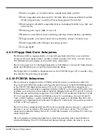
CMD's complete set of 32-bit drivers handle both DMA and PIO
♦
Fully compatible with the latest PCI, PCI IDE, ATA-2, Enhanced IDE, Fast IDE,
ATAPI, plug and play, and ATA-2 Power Management Feature Set
♦
Fully supports all ATAPI-compatible devices, including CD-ROM, tape, MO, and
other devices
♦
Fully supports legacy (IRQ 14 and 15)
♦
Hardware and software mode switching and chip enable/disable capabilities
♦
Programmable read-ahead and write-back buffers enhance transfer rates
♦
Fully compatible with all major operating systems
♦
100-pin PQFP
4.2.9 Floppy Disk Drive Subsystem
The Extensa 900 is equipped with a 3.5-inch floppy disk drive that can read/write
standard 3.5-inch disks (either1.44 MB or 2 MB capacity). The drive can also read a
720 KB disk (for interchange of data with other computers).
The data transfer rate for the floppy disk drive is 500 Kbits per second for high-density
disks and 250 Kbits per second for double-density disks.
The floppy drive controller is implemented on the PC87338 Super I/O Controller chip
described in the previous paragraphs.
4.2.10 PCMCIA Subsystem
The notebook is equipped with a PCMCIA subsystem that accomodates either two
Type I or Type II PCMCIA cards or one Type III card. The heart of the PCMCIA Subsystem
is the TI PCI 1130 high-performance PCI-to-PC Card controller that supports two
independent PC Card sockets compliant with the 1995 PC card standard. The PCI 1130
provides a set of features that make it ideal for bridging between PCI and PC Cards in
both notebook and desktop computers. The 1995 PC Card standard retains the 16-bit
PC Card specification defined in PCMCIA release 2.1 and defines the new 32-bit PC
Card, called CardBus, capable of full 32-bit data transfers at 33 MHz. The PCI 1130
supports any combination of 16-bit and CardBus PC Cards in its two sockets, powered
at 3.3V or 5V as required.
The PCI 1130 is compliant with the PCI local bus specification revision 2.1, and its PCI
interface can act as either a PCI master device or a PCI slave device. The PCI bus
mastering is initiated during 16-bit PC Card DMA transfers or CardBus PC Card bus
mastering cycles.
All card signals are internally buffered to allow hot insertion and removal without
external buffering. The PCI 1130 internal data path logic allows the host to access
Summary of Contents for Extensa 900 Series
Page 1: ...Maintenance Manual ExtensaTM 900 Series Notebook Computers 9813715 0001 December 1996 ...
Page 10: ......
Page 28: ......
Page 44: ......
Page 56: ......
Page 82: ......
Page 98: ......
Page 138: ...A 2 Notebook Schematic Diagrams Figure A 1 Notebook Main Board Logic Diagrams Sheet 1 of 30 ...
Page 139: ...Notebook Schematic Diagrams A 3 Figure A 1 Notebook Main Board Logic Diagrams Sheet 2 of 30 ...
Page 140: ...A 4 Notebook Schematic Diagrams Figure A 1 Notebook Main Board Logic Diagrams Sheet 3 of 30 ...
Page 141: ...Notebook Schematic Diagrams A 5 Figure A 1 Notebook Main Board Logic Diagrams Sheet 4 of 30 ...
Page 142: ...A 6 Notebook Schematic Diagrams Figure A 1 Notebook Main Board Logic Diagrams Sheet 5 of 30 ...
Page 143: ...Notebook Schematic Diagrams A 7 Figure A 1 Notebook Main Board Logic Diagrams Sheet 6 of 30 ...
Page 145: ...Notebook Schematic Diagrams A 9 Figure A 1 Notebook Main Board Logic Diagrams Sheet 8 of 30 ...
Page 146: ...A 10 Notebook Schematic Diagrams Figure A 1 Notebook Main Board Logic Diagrams Sheet 9 of 30 ...
Page 147: ...Notebook Schematic Diagrams A 11 Figure A 1 Notebook Main Board Logic Diagrams Sheet 10 of 30 ...
Page 148: ...A 12 Notebook Schematic Diagrams Figure A 1 Motherboard PWB Logic Diagrams Sheet 11 of 23 ...
Page 149: ...Notebook Schematic Diagrams A 13 Figure A 1 Notebook Main Board Logic Diagrams Sheet 12 of 30 ...
Page 153: ...Notebook Schematic Diagrams A 17 Figure A 1 Notebook Main Board Logic Diagrams Sheet 16 of 30 ...
Page 154: ...A 18 Notebook Schematic Diagrams Figure A 1 Notebook Main Board Logic Diagrams Sheet 17 of 30 ...
Page 155: ...Notebook Schematic Diagrams A 19 Figure A 1 Notebook Main Board Logic Diagrams Sheet 18 of 30 ...
Page 156: ...A 20 Notebook Schematic Diagrams Figure A 1 Notebook Main Board Logic Diagrams Sheet 19 of 30 ...
Page 157: ...Notebook Schematic Diagrams A 21 Figure A 1 Notebook Main Board Logic Diagrams Sheet 20 of 30 ...
Page 158: ...A 22 Notebook Schematic Diagrams Figure A 1 Notebook Main Board Logic Diagrams Sheet 21 of 30 ...
Page 159: ...Notebook Schematic Diagrams A 23 Figure A 1 Notebook Main Board Logic Diagrams Sheet 22 of 30 ...
Page 160: ...A 24 Notebook Schematic Diagrams Figure A 1 Notebook Main Board Logic Diagrams Sheet 23 of 30 ...
Page 161: ...Notebook Schematic Diagrams A 25 Figure A 1 Notebook Main Board Logic Diagrams Sheet 24 of 30 ...
Page 166: ...A 30 Notebook Schematic Diagrams Figure A 1 Notebook Main Board Logic Diagrams Sheet 29 of 30 ...
Page 168: ......
Page 171: ...MPB Schematic Diagrams B 3 Figure B 1 MPB CPU Board Logic Diagrams Sheet 2 of 3 ...
Page 176: ...B 8 MPB Schematic Diagrams Figure B 3 MPB Main Board Motherboard Logic Diagrams Sheet 3 of 10 ...
Page 196: ......
Page 197: ......
Page 198: ......


