

Acer V551 (new) CRT Monitor Service Guide
Chapter 2 Circuit Operation Theory
15
Confidence and Property
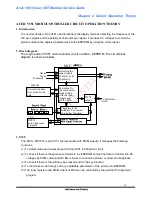
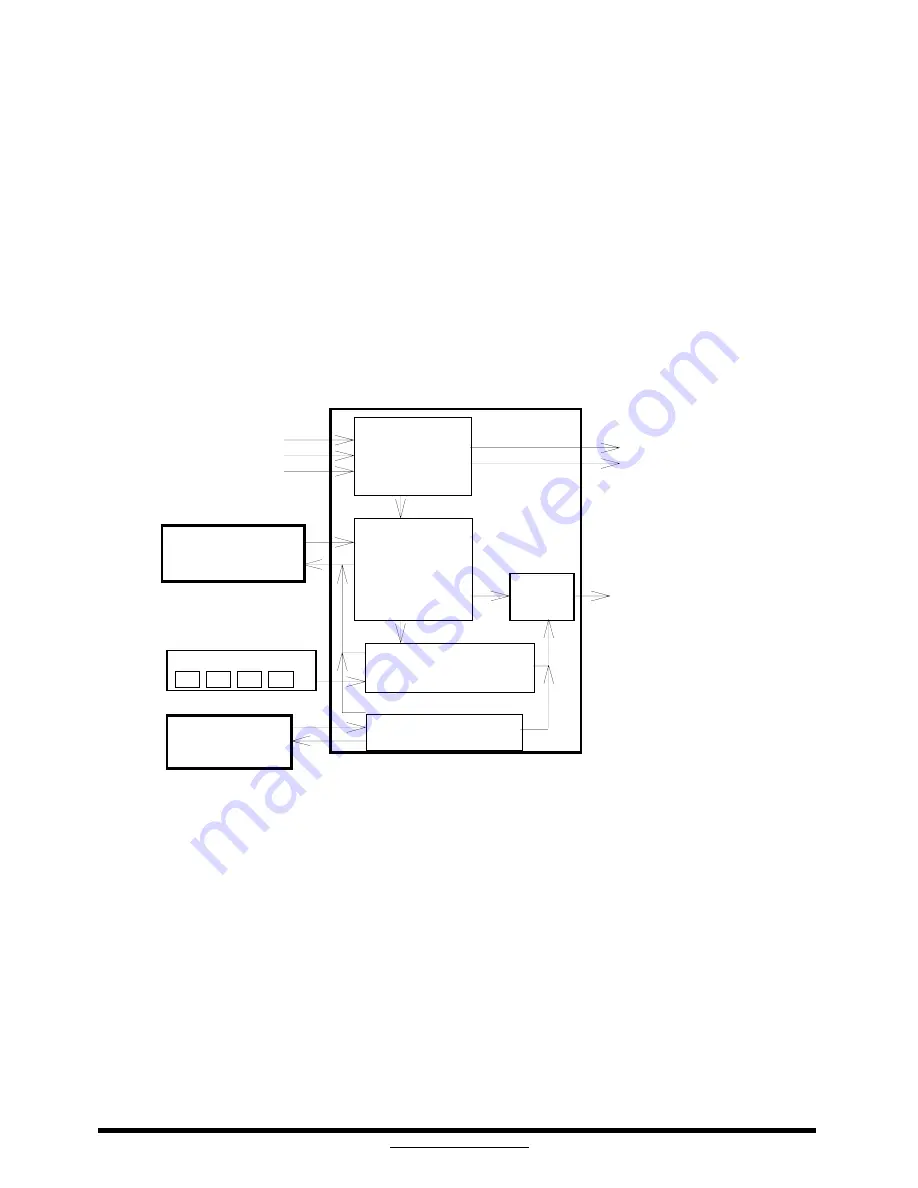
ACER V551 MICROCONTROLLER CIRCUIT OPERATION THEORY
1. Introduction
The microcontroller of the V551 can discriminate the display mode by detecting the frequency of the
H/V sync signals and the polarity of horizontal sync signal. It provides DC voltages to control the
picture and save the adjusted parameters into the EEPROM by using the control panel.
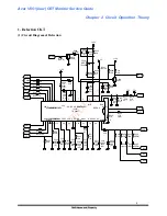
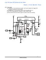
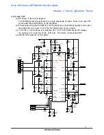
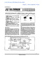
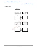
2. Block diagram
The major parts of V551 microcontroller circuit are MCU, EEPROM. The circuit block
diagram is shown as below,
MCU
Hsync
Vsync
H-polarity
Preset mode data,
User saved mode
data.
Searching for
the same saved
mode timing
with the input
signals and
get the data.
Detecting the
input signals
of H,Vsync &
H-polarity.
Checking if the
valid key be pressed
and do key function.
PWM
output
To deflection
circuit
PC
RS232
auto alignment
program
EEPROM
Blanking
Blanking
Blanking
Blanking
SCO-SC
1
SCO-SC
1
SCO-SC
1
SCO-SC
1
Control Panel
Control Panel
Control Panel
Control Panel
Select Adjust
Select Adjust
Select Adjust
Select Adjust
-
--
-
-
--
-
+
++
+
+
++
+
(UART) External
(UART) External
(UART) External
(UART) External
adjustment function
adjustment function
adjustment function
adjustment function
(MTV0
1
2)
(MTV0
1
2)
(MTV0
1
2)
(MTV0
1
2)
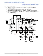
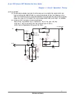
3. MCU
The MCU - MTV012 is an 87C51 microcontroller with PWM outputs. It manages the following
functions,
(1) To detect mode and output proper SC0 and SC1 to deflection circuit.
(2) To check if there is the same saved mode in the EEPROM and get the data to transfer into DC
voltages by PWM output and RC filter circuits to control the picture, contrast and brightness.
(3) To check if there is the valid key be pressed and do the key function.
(4) To memorize mode timings and any adjustable parameters of the picture into EEPROM.
(5) The inner registers and PWM output of MCU can be controlled by the external PC alignment
program.


