PCIe Accelerator-6D Card User Guide (UG074)
Speedster FPGAs
31
Switches
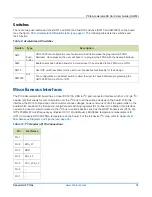
There are two push-button switches (SW1 and SW2) and two DIP switches (SW10 and SW3000) on the board
(see the figure,
. The following table lists the switches and
PCIe Accelerator-6D Board Details) (see page 9)
their function:
Table 9:
Accelerator-6D Switches
Switch
Type
Description
SW1
Push
button
HD1000 FPGA configuration reset switch which will reset/erase the programmed FPGA
bitstream. Once pressed, the user will have to re-program the FPGA with the desired bitstream.
SW2
Board reset switch which allows for a manual reset to be provided to the FPGA via a GPIO.
SW10
DIP
User DIP switch available for the user to set the desired functionality for their design.
SW3000
The configuration mode select switch to allow the user to choose between programming the
HD1000 FPGA via JTAG or SPI.
Miscellaneous Interfaces
The PCIe Accelerator-6D board has a Linear DC1613A USB to I C pod connector interface which is a 12-pin I C
2
2
header (J3) that allows for communication over the I C bus to all the various devices on the board. With this
2
interface, the DC1613A pod can control/monitor various voltages, power and current of all the power rails on the
board which are driven by their power controller and switching regulator ICs on-board. In addition, this interface
can also be used to communicate via the I C bus to various devices such as the QSFP transceivers (U116, J5),
2
IDT's 8T49N287 clock frequency synthesizer IC (U12) and Maxim's MAX6642 temperature measurement IC
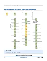
(U31) to measure HD1000 FPGA temperature on the board. For the full device I C map, refer to
2
Miscellaneous Diagrams and Figures (see page 36)
Table 10:
I C Header (J3) Pin Connections
2
Pin
Net Name
Pin 1
–
Pin 2
SDA_LT
Pin 3
GND
Pin 4
SCL_LT
Pin 5
VCC_3V3_LT
Pin 6
–
Pin 7
–


