42
42
-
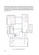
Input sensor board (located on the Capacitors board);
-
Inductors board;
-
Capacitors board;
-
Output sensor and antenna switch board;
-
Control board (includes modem, four service LEDs and two buttons).
The matching RF circuit is an L-shape matching network configuration and is com
-
prised of the Capacitors board and Inductors board.
The Inductors board contains 9 discrete coils that can be bypassed or added in series
by relays KL1 to KL9. Together, they form an inductor with a maximum value of over
6.25uH, variable in 0.015uH increments. The discretely controlled inductor is connect
-
ed in series between the tuner input (to the transmitter) and output (to the antenna).
The Capacitor board contains 10 discrete capacitors that can be switched off or con
-
nected in parallel by relays KC1 to KC10. Together, they form a capacitor with a maxi
-
mum value of over 2800pF, variable in 3pF increments.
The discretely controlled capacitor can be connected in parallel to the tuner input (from
the transmitter) or to the output (to the antenna) using two relays: KCT and KCA, re-
spectively, forming the two basic configurations of an L or reverse L matching network,
required for the different antenna impedances:
-
L-network (KCT on, KCA off) – for matching of mainly low impedances
-
Reverse L-network (KCT off, KCA on) – for matching mainly high impedances.
After the matching circuit, the RF power passes through the output sensor and the an-
tenna switch, reaching the selected antenna output (1 of 4). The output sensor produc-
es four analog signals for the output forward and reflected power, antenna current and
antenna voltage: fwda, rfla, ia, and ua. The antenna switch is controlled by four relays,
KA1 to KA4. There is a lightning surge arrestor (not shown in the block diagram) at the
output sensor to protect the tuner and the devices connected to it from atmospheric
discharges.
The input RF power from the amplifier, along with the +26VDC power supply and the
modem 60kHz control signal is fed to the input switch board, at the RF Input connector.
Here, by using suitable filters, the 60kHz modem signal is separated and fed to and
from the Control board. The power 26VDC is separated and used to derive
a +5V power supply and three auxiliary DC voltages: +180V, +12V, and -12V for the
MOSFET INPUT SWITCH. The CROWBAR relay has a protection function and is nor-
mally open. The +180V auxiliary voltage is enabled and disabled by the HVON signal
from the Control board.
During tuner operation (after tuning), in normal state of the relays KS1 and KS2, the
input RF power is directly fed from the RF Input to the input of the L matching network.
During the basic cycle of tuning, by switching the KS1 relay over to the Input switch
MOSFET, the input RF power is directed through a 27 Ohm/100W resistor to the tran-
sistor MOSFET INPUT SWITCH and to the TUN input of the Sensor board. In this
Summary of Contents for ACOM 04AT
Page 1: ...1 ...
Page 57: ...2 2 ...

