background image

ACEX4041 COM Express Type 10 

AcroPack Carrier Board 

- 29 - 

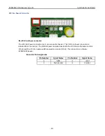
Connector Pin assignments


Carrier 

J6, J7 and 

Termination 

Panel 

Carrier 

P1, P2, P3, and P4 

Samtec 

SS5-50-3.00-L-D-K-TR 

Module Pin 

Number 

Field I/O Signal 

Field I/O 1 

35 

Field I/O 2 


Reserved/isolation 


Reserved/isolation 

Field I/O 3 

36 

Field I/O 4 


Reserved/isolation 


Reserved/isolation 

10 

10 

Field I/O 5 

37 

Field I/O 6 


12 

12 

Reserved/isolation 


11 

11 

Reserved/isolation 

14 

14 

Field I/O 7 

38 

13 

13 

Field I/O 8 


16 

16 

Reserved/isolation 


15 

15 

Reserved/isolation 

18 

18 

Field I/O 9 

39 

17 

17 

Field I/O 10 


20 

20 

Reserved/isolation 


19 

19 

Reserved/isolation 

22 

22 

Field I/O 11 

40 

21 

21 

Field I/O 12 


24 

24 

Reserved/isolation 


23 

23 

Reserved/isolation 

26 

26 

Field I/O 13 

41 

25 

25 

Field I/O 14 


28 

28 

Reserved/isolation 


27 

27 

Reserved/isolation 

30 

30 

Field I/O 15 

42 

29 

29 

Field I/O 16 


32 

32 

Reserved/isolation 


31 

31 

Reserved/isolation 

34 

34 

Field I/O 17 

43 

33 

33 

Field I/O 18 

Summary of Contents for ACEX4041

Page 1: ...ack Carrier Board USER S MANUAL ACROMAG INCORPORATED 30765 South Wixom Road Wixom MI 48393 2417 U S A Tel 248 295 0310 Copyright 2019 Acromag Inc Printed in the USA Data and specifications are subject...

Page 2: ...ows 8 VxWorks 8 Linux 8 2 PREPARATION FOR USE 9 UNPACKING AND INSPECTION 9 BOARD CONFIGURATION 10 COM Express Type 10 CPU Site 11 SATA Interface 16 Serial Interface 17 Audio Interface 18 CPU Fan Power...

Page 3: ...40 40 40 40 FIELD GROUNDING CONSIDERATIONS 41 3 PROGRAMMING INFORMATION 41 4 THEORY OF OPERATION 42 FUNCTIONAL BLOCK DIAGRAM 42 COM Express Type 10 Mini interface 43 PCIe Switch Clock Buffer 43 AcroPa...

Page 4: ...s Type 10 AcroPack Carrier Board 4 Reliability Prediction 48 7 Appendix 49 Battery Backup Mode setup 49 I O Panel with overlay accessory 51 Cables and Accessories 52 8 CERTIFICATE OF VOLATILITY 53 9 R...

Page 5: ...d All other trademarks registered trademarks trade names and service marks are the property of their respective owners Radio Frequency Interference Statement This is a Class A product In a domestic en...

Page 6: ...ector and a SATA power connector to allow for use of a Solid State Disk Drive Mini Display Port High resolution graphics interface connection Audio Interface Provides interface Line in Line out throug...

Page 7: ...Resettable PTC fuse is present on each supply line serving each AcroPack module except for the 3 3V Fuse The 3 3V Fuse is A Fast Acting Surface Mount Fuse SMF and is a small 1206 size thin film device...

Page 8: ...eads writes of registers and the writing of interrupt handlers VxWorks Acromag provides a software product sold separately consisting of VxWorks software This software Model APSW API VXW is composed o...

Page 9: ...ields unless the device is contained within its original manufacturer s packaging Be aware that failure to comply with these guidelines will void the Acromag Limited Warranty UNPACKING AND INSPECTION...

Page 10: ...ACEX4041 COM Express Type 10 AcroPack Carrier Board 10 BOARD CONFIGURATION ACEX4041 PCB Mini ITX Form Factor 170mm x 170mm...

Page 11: ...ctor This site supports the COM Computer on Module Express Type 10 Mini CPU Module form factor 84mm x 55 mm CPU Modules with A Single 220 Pin A B COM Express Connector NOTE The CPU Modules are typical...

Page 12: ...CONNECT1 LPC_CLK 11 GND GND 12 NO CONNECT1 PWRBTN 13 NO CONNECT1 SMB_CK 14 NO CONNECT1 SMB_DAT 15 SUS_S3 SMB_ALERT 16 SATA0_TX SATA1_TX 17 SATA0_TX SATA1_TX 18 SUS_S4 NO CONNECT1 19 SATA0_RX SATA1_RX...

Page 13: ...NNECT1 NO CONNECT1 43 NO CONNECT1 NO CONNECT1 44 NO CONNECT1 USB_0_1_OC 45 USB0 USB1 46 USB0 USB1 47 VCC_RTC NO CONNECT1 48 NO CONNECT1 NO CONNECT1 49 NO CONNECT1 SYS_RESET 50 NO CONNECT1 CB_RESET 51...

Page 14: ...ECT1 NO CONNECT1 80 GND GND 81 NO CONNECT1 DDIO_PAIR3 82 NO CONNECT1 DDIO_PAIR3 83 NO CONNECT1 NO CONNECT1 84 NO CONNECT1 VCC_5V_SBY 85 GPI3 VCC_5V_SBY 86 RSVD2 VCC_5V_SBY 87 NO CONNECT1 VCC_5V_SBY 88...

Page 15: ..._12V 107 VCC_12V VCC_12V 108 VCC_12V VCC_12V 109 VCC_12V VCC_12V 110 GND GND For detailed signal descriptions refer to the COM Express Module Base Specification Rev 2 1 Note 1 NO CONNECT The functiona...

Page 16: ...en on the carrier and must be installed to bring 3 3V power to pin 3 of this connector This connector is a Molex 470531000 header Connector Pin Assignments Pin Number Signal Name Pin Number Signal Nam...

Page 17: ...Signal Name Function 1 NC No connect 2 NC No connect 3 RX Receive 4 TX Transmit 5 GND Ground 6 GND Ground P9 Serial Port connector The Serial Port is General Purpose Serial Port capable of driving TTL...

Page 18: ...Right channels for output and Line In left and right for Input There are 2 Line In signals and 2 Line out signals and 2 grounds The Audio Port is labeled P13 The connector is a Molex 55932 0610 socket...

Page 19: ...nductor header The CPU Fan Power connector is labeled P6 on the carrier The COM Express module drives both the CPU Fan tachometer control Pin 3 and the CPU Fan pulse width modulation control Pin 4 Thi...

Page 20: ...the AcroPack modules The connector is a Molex 87832 1420 Connector Pin Assignments Notes NC no connect TMS JTAG Test Mode Select This pin is the JTAG mode signal establishing appropriate TAP state tr...

Page 21: ...mates with the power supply connector Molex 39 01 2240 or equivalent For more information view the ATX Specification Ver 2 2 Connector Pin Assignments Notes 1 NC no connect Pin Number Signal Name Pin...

Page 22: ...ignal from the COM Express module to the outside world when the carrier is mounted in side an enclosure When this signal is brought to a logic low the system will turn on Pin 3 of this connector can b...

Page 23: ...rts sizes 2242 2260 and 2280 For more information about M 2 see the PCI SIG PCI Express M 2 Specification 1 0 or later Connector Pin Assignments Pin Number Signal Name Pin Number Signal Name 1 GND 2 3...

Page 24: ...Name Pin Number Signal Name 51 GND 52 NC1 53 NC1 54 NC1 55 NC1 56 NC1 57 GND 58 NC1 59 Mechanical key 60 Mechanical key 61 Mechanical key 62 Mechanical key 63 Mechanical key 64 Mechanical key 65 Mech...

Page 25: ...cification with the exceptions noted below in the following table Also see important Mini PCIe usage information below Connector Pin Assignments Pin Number Signal Name Pin Number Signal Name 1 N C WAK...

Page 26: ...tion for additional power connections If you are installing a Mini PCIe card from another manufacturer in slot A remove fuses F6 5V F7 12V and F8 12V When installing a Mini PCIe card in from another m...

Page 27: ...elf resetting fuses AcroPack site A Signal Name F6 5V F7 12V F8 12V F9 1 5V F10 3 3V AcroPack site B Signal Name F16 5V F17 12V F18 12V F19 1 5V F20 3 3V AcroPack site C Signal Name F21 5V F22 12V F23...

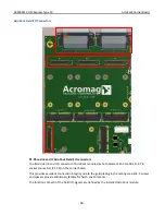
Page 28: ...nector of AcroPack modules mate to Samtec SS5 50 3 00 L D K TR socket connectors P1 P4 on the carrier board This provides excellent connection integrity due to the gold plating in the mating area M2 5...

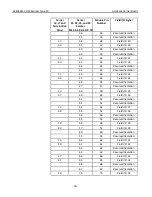
Page 29: ...d I O 5 37 9 9 Field I O 6 12 12 Reserved isolation 11 11 Reserved isolation 4 14 14 Field I O 7 38 13 13 Field I O 8 16 16 Reserved isolation 15 15 Reserved isolation 5 18 18 Field I O 9 39 17 17 Fie...

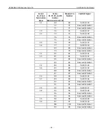
Page 30: ...rved isolation 12 46 46 Field I O 23 46 45 45 Field I O 24 48 48 Reserved isolation 47 47 Reserved isolation 13 50 50 Field I O 25 47 49 49 Field I O 26 52 52 Reserved isolation 51 51 Reserved isolati...

Page 31: ...eld I O 39 54 77 77 Field I O 40 80 80 Reserved isolation 79 79 Reserved isolation 21 82 82 Field I O 41 55 81 81 Field I O 42 84 84 Reserved isolation 83 83 Reserved isolation 22 86 86 Field I O 43 5...

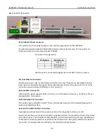
Page 32: ...ected J8 Dual USB 3 0 connector USB 3 0 ports support speed of 5Gb s Port one is on the bottom and port 2 is on the top This is a standard USB 3 0 connection J9 Mini Display Port Connector This is als...

Page 33: ...configuration settings of the CPU module The Super Cap will keep the RTC and CMOS voltages up for approximately 3 full Days without any power applied to the ACEX4041 The actual time the Super Cap will...

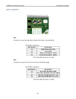
Page 34: ...al Time Clock CMOS external battery option Pin 1 Positive 3V Pin 2 Negitive Ground Mating connector JST Sales America inc P N PHR 2 CONN HOUSING PH 2POS 2MM WHITE POST CODE Display A two digit LED dis...

Page 35: ...ch is used for CPLD functions for the POST CODE Display Switch SW2 assignments The Factory default position is in bold SW1 Position Signal Name 1 2 CMOS Normal Operation 2 3 Clear CMOS 4 5 Battery Bac...

Page 36: ...ACEX4041 COM Express Type 10 AcroPack Carrier Board 36 Switch 3 and Switch 4 SW3 Power Momentary switch to power system on and off SW4 Reset Momentary switch to restart the system...

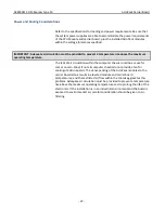
Page 37: ...lack of air circulation within the computer chassis could be a cause for some concern Most if not all computer chassis do not provide a fan for cooling of add in boards The dense packing of the AcroPa...

Page 38: ...l align the COM Express connector of the Module with the COM express connector on the Carrier 2 Carefully press the CPU module straight down until the CPU COM Express connector seats into the COM Expr...

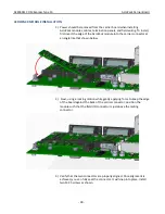
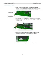
Page 39: ...module into the carrier connector at an angle like that shown below 2 Next using a rocking motion while gently applying force to keep the edge of the board against the back of the carrier connector po...

Page 40: ...lder screw and the nylon washer from the carrier 2 Insert the edge of the AcroPack module into the carrier connector at an angle like that shown below Also place the washer in the size location for yo...

Page 41: ...ut isolation to avoid ground loops and noise pickup This is particularly important for analog I O applications when a high level of accuracy resolution is needed 12 bits or more Contact your Acromag r...

Page 42: ...ACEX4041 COM Express Type 10 AcroPack Carrier Board 42 4 THEORY OF OPERATION FUNCTIONAL BLOCK DIAGRAM...

Page 43: ...6 independent x1 ports one for each AcroPack site and one for each Ethernet controller The host port consists of four PCIe lanes x4 port AcroPack sites and Ethernet controllers have one lane x1 port e...

Page 44: ...SSD Socket 2 mechanical Key B and for modules that are SSD Socket 3 mechanical key M This site supports sizes 2242 2260 and 2280 For more information about M 2 see the PCI SIG PCI Express M 2 Specifi...

Page 45: ...o the Support tab to access Application Notes White Papers I O Questions Answered Acromag s application engineers can also be contacted directly for technical assistance via email or telephone through...

Page 46: ...ket Molex 67800 800 P8 Serial Port 6 pin header Molex 55932 0610 P9 Serial Port 6 pin header Molex 55932 0610 P13 Audio 6 pin header Molex 55932 0610 P6 Fan Power 4 pin header Molex 470531000 P14 Exte...

Page 47: ...and F18 12V for slot B F22 12V F21 5V and F23 12V for slot C and F12 12V F13 5V and F11 12V for slot D Littelfuse 1206L110 12SL Other Fuses 10 36Vdc 8 Amps F4 DC Input Littelfuse 0451008 MRL Mini Dis...

Page 48: ...Designed to comply with IEC 60068 2 64 10 500Hz 5G rms 2 Hours axis Shock Operating Designed to comply with IEC 60068 2 27 30G 11ms half sine 50G 3mS half sine 18 shocks at 6 orientations for both te...

Page 49: ...10 AcroPack Carrier Board 49 7 Appendix Battery Backup Mode setup To enable Battery Backup Mode change switch 1 to 4 5 position as shown Connect ATX power supply to the 24 Pin ATX connector This will...

Page 50: ...arging the Battery Battery Backup operation The ACEX4041 is powered by the ATX power supply If loss of AC power to the ATX power supply occurs the Battery will automatically start delivering power to...

Page 51: ...er Board 51 I O Panel with overlay accessory Installation Remove the 8 jackscrews from the field I O connectors on the ACEX4041 PCB Install the rear panel onto the ACEX4041 PCB Secure by installing th...

Page 52: ...420 Round cable shielded male SCSI 3 connector to 68 pin CHAMP 08mm 2 meters long 5028 615 APIO CABLE 68 PIN CHAMP PIGTAIL 36 INCH 5028 616 APIO CABLE 68 PIN CHAMP PIGTAIL 70 INCH 5028 617 ACEX4041 C...

Page 53: ...mory of whose contents is retained when power is removed Yes No Type EEPROM FLASH etc Size User Modifiable Function Process to Sanitize FLASH 1 Mbit Yes PCIe switch configuration Overwrite FLASH conte...

Reviews: