SERIES AP440 ACROPACK
USER
’S MANUAL
Acromag, Inc. Tel: 248-295-0310
- 20 - http://www.acromag.com
- 20 -
www.acromag.com
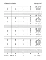
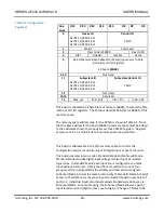
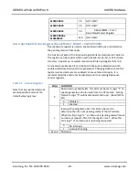
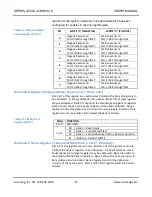
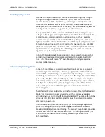
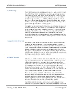
Table 3.2: Standard Mode
Memory Map
Notes:
1. These are Read Only
registers
2. The AP will respond to
addresses that are “Not
Used”. The board will
return “0” for all address
reads that are not used or
reserved.
3. Writing four unique bytes
(07H, 0DH, 06H, and 12H)
to port 7, in consecutive
order, will switch to
Enhanced Mode. Perform
this operation after reset or
power-up with interrupts
disabled. Do not read or
write to any other port
between writes.
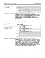
BAR0 Base Address
Bit(s)
Description
0x0000 0000
7:0
Interrupt Register
0x0000 0004
7:0
Location in System Register
0x0000 0008
7:0
READ
1
– Port 0
Register IN00-IN07
0x0000 000C
7:0
READ
1
– Port 1
Register IN08-IN15
0x0000 0010
7:0
READ
1
– Port 2
Register IN16-IN23
0x0000 0014
7:0
READ
1
– Port 3
Register IN24-IN31
0x0000 0018
7:0
NOT USED
2
0x0000 001C
7:0
NOT USED
2
0x0000 0020
7:0
NOT USED
2
0x0000 0024
7:0
READ/WRITE - Port 7
ENHANCED MODE SELECT REGISTER
3
0x0000 0028→
0x00000040
31:0
NOT USED
2
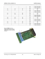
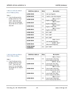
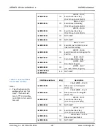
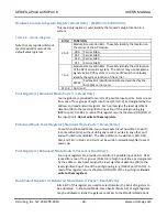
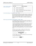
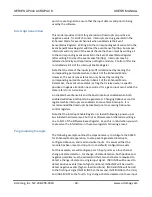
Table 3.3: Registers in
Standard and Enhanced Mode
Memory Map
Notes:
1. These registers are
addressable in both
Standard and Enhanced
mode in all banks 0 to 2.
2. The AP will respond to
addresses that are “Not
Used”. The board will
return “0” for all address
reads that are not used or
reserved.
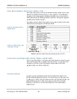
BAR0 Base Address
Bit(s)
Description
0x0000 0044
7:0
READ/WRITE – Port 1
Software Reset Generator (Bit 1 = 1
Generates Reset)
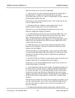
0x0000 0048
15:0
XADC Status/Control Register
0x0000 004C
15:0
XADC Address Register
0x0000 0050→
0x000001FC
31:0
NOT USED
2
0x0000 0200
31:0
Firmware Revision
0x0000 0204
7:0
Flash Data
0x0000 0208
Bit-0
Flash Chip Select
0x0000 020C→
0x000007FF
31:0
NOT USED
2

