SERIES AP440 ACROPACK
USER
’S MANUAL
Acromag, Inc. Tel: 248-295-0310
- 28 - http://www.acromag.com
- 28 -
www.acromag.com
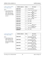
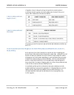
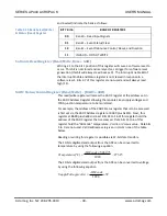
Table 3.16 Bank Select
Register (Read)
Bit(s)
FUNCTION
5 to 0
NOT USED
7 to 6
00
Bank 0 – Read Inputs
01
Bank 1 – Event Status/Clear
10
Bank 2 – Event Debounce Control, Reset, & Duration
11
INVALID – DO NOT WRITE
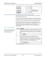
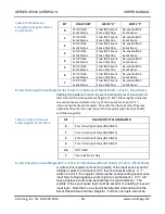
Debounce Control Register (Enhanced Mode Bank 2, Port 0, Read/Write)
This register is used to control whether each individual port is to be passed
through the debounce logic before being recognized by the circuitry. A “0”
disables the debounce logic, and a “1” enables the debounce logic.
Debounce applies to both inputs and event sense inputs, and only in
Enhanced Mode.
Furthermore after enabling the debounce circuitry, wait at least three times
the programmed debounce duration prior to reading the input ports or
event signals to insure valid data.
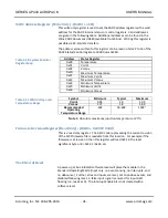
Table 3.17 Debounce Control
Register
Note that any registers/bits not
mentioned will remain at the
default value logic low.
Bit(s)
FUNCTION
0
Port 0 (IN00-IN07) Debounce Control
0
Disabled
1
Enabled
1
Port 1 (IN08-IN15) Debounce Control
0
Disabled
1
Enabled
2
Port 2 (IN16-IN23) Debounce Control
0
Disabled
1
Enabled
3
Port 3 (IN24-IN31) Debounce Control
0
Disabled
1
Enabled
7 to 4
Not Used
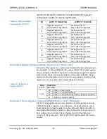
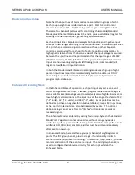
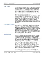
Debounce Duration Register 0 (Enhanced Mode Bank 2, Port 1, Read/Write)
This register controls the duration required by each input signal before it is
recognized by each individual ASIC input in the Enhanced Mode. Register 0
controls debounce for ports 0-3. If the debounce clock has been selected
(see Debounce Clock Select Register), then the 31.25MHz internal system
clock will allow the debounce times shown below to be selected (actual
times vary to within minus 25% of nominal). Note that this time applies to
the ASIC input and does not include the optocoupler time delay.


