SERIES AP440 ACROPACK
USER
’S MANUAL
Acromag, Inc. Tel: 248-295-0310
- 31 - http://www.acromag.com
- 31 -
www.acromag.com
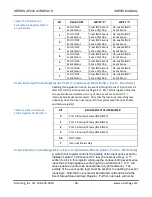
XADC Address Register (Write Only) - (BAR0 + 4CH)
This write only register is used to set the XADC address register with a valid
address for the XADC internal status or control registers. Valid addresses
are given in the following table. Additional addresses can be found in the
Xilinx XADC document UG480 (available from Xilinx). Writing this register is
possible via 32-bit data transfers.
The address value written to this register can be read on bits 22 to 16 of the
XADC Status/Control register at BAR0 plus 0x48H.
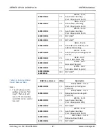
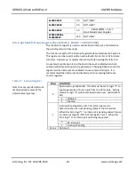
Table 3.20: System Monitor
Register Map
Address
Status Register
0x00
Temperature
0x01
Vccint
0x02
Vccaux
0x20
Maximum Temperature
0x21
Maximum Vccint
0x22
Maximum Vccaux
0x24
Minimum Temperature
0x25
Minimum Vccint
0x26
Minimum Vccaux
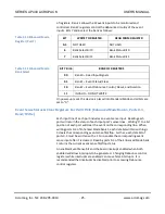
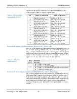
Table 3.21 FPGA Voltage and
Temperature Range
Symbol
Minimum
Typical
Maximum
Vccint
0.95
1.0
1.05
Vccaux
1.71
1.8
1.89
Recommended
Operating
Temperature Range
-40C
50-60C
100C
1
Note 1: Absolute maximum junction temperature 125
o
C.
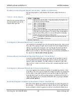
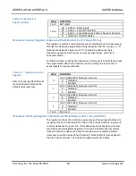
Firmware Revision Register (Read Only) - (BAR0 + 0x0000 0200)
This is a read only register. The ASCII code representing the current revision
of the MCS firmware file is readable from this location. For example if the
firmware is at revision A then this register will read 0x41 in the least
significant byte or B= 0x42, C=0x43, etc.
The Effect of Reset
A power-up or bus-initiated software reset will place the module in the
Standard Operating Mode (input only, no event sensing, no interrupts, and
no debounce). Further, all event inputs are reset, set to positive events, and
disabled following reset. A false input signal is ensured for inputs left
floating (i.e. reads as 0). The Interrupt Enable bit is not cleared with a
software reset.

