SERIES AP440 ACROPACK
USER
’S MANUAL
Acromag, Inc. Tel: 248-295-0310
- 30 - http://www.acromag.com
- 30 -
www.acromag.com
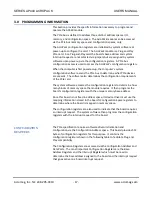
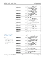
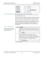
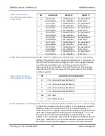
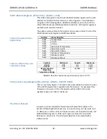
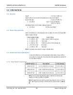
and 6 select/indicate the bank as follows:
Table 3.19 Bank Select (Write)
& Status (Read) Register
BIT 7 Bit 6
BANK OF REGISTERS
00
Bank 0 – Read Input Signals
01
Bank 1 – Event Status/Clear
10
Bank 2 – Event Debounce Control, Reset, and Duration
11
INVALID – DO NOT WRITE
Software Reset Register (Read/Write, Base + 44H)
Writing a 1 to the bit 1 position of this register will cause a software reset to
occur. This bit is not stored and merely acts as a trigger for software reset
generation (this bit will always read back as 0). The Interrupt Enable Bit of
the Interrupt Enable and Status register is not cleared in response to a
software reset. Bits 2-7 of this register are not used and will always read
high (1’s).
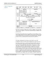
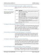
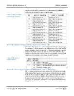
XADC Status/Control Register (Read/Write) - (BAR0 + 48H)
This read/write register will access the XADC register at the address set in
the XADC Address Register allowing the module’s key supply voltages and
FPGA junction temperature to be monitored.
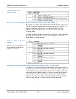
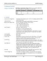
For example, the address of the XADC Status register that is to be accessed
is first set via the XADC Address register at BAR0 plus 0x4CH. Next, this
register at BAR0 plus 0x48H is read. Bits 22 to 16 of this register hold the
address of the XADC register that is accessed. Data bits 15 to 6 of this
register hold the “ADCcode” temperature, Vccint, or Vccaux value. Data bits
5 to 0 are not used. Valid addresses are given in column one of the table
below.
Reading or writing this register is possible via 32-bit data transfers.
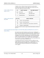
The 10-bits digitized and output from the ADC can be converted to
temperature by using the following equation.
15
.
273
1024
975
.
503
)
(
ADCcode
C
e
Temperatur
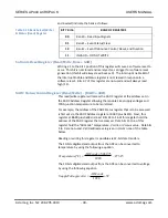
The 10-bits digitized and output from the ADC can be converted to voltage
by using the following equation.
V
ADCcode
volts
age
SupplyVolt
3
1024
)
(


