SERIES AP470 ACROPACK
USER
’S MANUAL
Acromag, Inc. Tel: 248-295-0310
- 17 -
http://www.acromag.com
- 17 -
www.acromag.com
CONFIGURATION REGISTERS
The PCIe specification requires software driven initialization and
configuration via the Configuration Address space. This board provides 512
bytes of configuration registers for this purpose. It contains the
configuration registers shown in the following table to facilitate Plug-and-
Play compatibility.
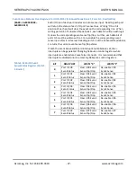
The Configuration Registers are accessed via the Configuration Address and
Data Ports. The most important Configuration Registers are the Base
Address Registers which must be read to determine the base address
assigned to the board and the Interrupt Register which must be read to
determine the interrupt request that goes active on a board interrupt
request.
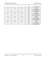
Table 3.1 Configuration
Registers
Reg.
Num.
D31 D24
D23 D16
D15 D8
D7 D0
0
Device ID
0x7016 AP470
Vendor ID
16D5
1
Status
Command
2
Class Code=118000
Rev ID=00
3
BIST
Header
Latency
Cache
4
64-bit Memory Base Address for Memory Accesses to PCIe
interrupt and I/O registers
4K Space (BAR0)
5:10
Not Used
11
Subsystem ID
0x7016 AP470
Subsystem Vendor ID
16D5
12
Not Used
13,14
Reserved
15
Max_Lat
Min_Gnt
Inter. Pin
Inter. Line
This board is allocated a 4K byte block of memory (BAR0), to access the PCIe
interrupt and I/O registers. The PCIe bus decodes 4K bytes for BAR0 for this
memory space.
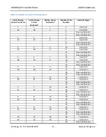
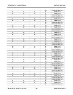
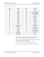
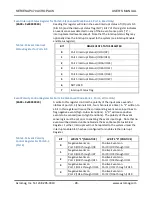
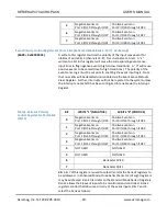
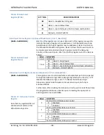
The memory space address map for the AP470 is shown in Table 3.2. Note
that the base address for the board (BAR0) in memory space must be added
to the addresses shown to properly access these AP470 registers. Register
accesses as 32, 16, and 8-bit data in memory space are permitted. All the
registers of the AP470 are accessed via data lines D0 to D31.

