SERIES AP220 / AP231 ACROPACK
USER
’S MANUAL
Acromag, Inc. Tel: 248-295-0310
- 16 -
http://www.acromag.com
- 16 -
https://www.acromag.com
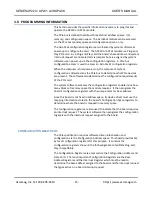
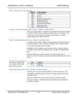
Table 3.1 Configuration Registers
Reg.
Num.
D31 D24
D23 D16
D15 D8
D7 D0
0
Device ID
0x701A AP220
0x701B AP231
Vendor ID
16D5
1
Status
Command
2
Class Code=118000
Rev ID=00
3
BIST
Header
Latency
Cache
4
64-bit Memory Base Address for Memory Accesses to PCIe
interrupt and I/O registers
4K Space
(BAR0)
5:10
Not Used
11
Subsystem ID
0x701A AP220
0x701B AP231
Subsystem Vendor ID
16D5
12
Not Used
13,14
Reserved
15
Max_Lat
Min_Gnt
Inter. Pin
Inter. Line
This board is allocated a 4K byte block of memory (BAR0), to access the PCIe
interrupt and I/O registers. The PCIe bus decodes 4K bytes for BAR0 for this
memory space.
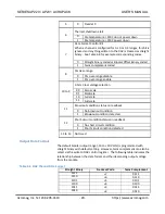
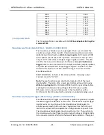
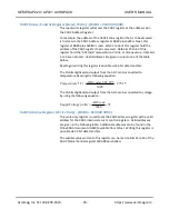
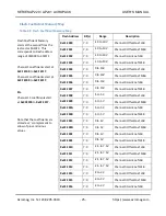
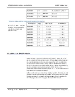
The memory space address map for the AP220 or AP231 is shown in Table
3.2. Note that the base address for the board (BAR0) in memory space must
be added to the addresses shown to properly access these AP220 and AP231
registers. Register accesses as 32, 16, and 8-bit data in memory space are
permitted. All the registers of the AP220 or AP231 are accessed via data
lines D0 to D31.
Table 3.2: BAR0 Registers
Note that any registers/bits not
mentioned will remain at the
default value logic low.
BAR0 Base Address
Bit(s)
Description
0x0000 0000
31:0
Not Used
0x0000 0004
7:0
Location in System Register
0x0000 0008
31:0
DAC Channel 0
0x0000 000C
31:0
DAC Channel 1
0x0000 0010
31:0
DAC Channel 2
0x0000 0014
31:0
DAC Channel 3

