background image

SERIES AP220 / AP231 ACROPACK 


USER

’S MANUAL 


Acromag, Inc. Tel: 248-295-0310  

            - 27 -                                   

http://www.acromag.com  

- 27 - 

https://www.acromag.com 


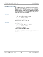
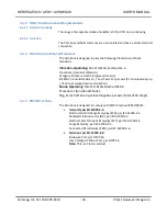
4.1   Uncalibrated Performance 


The uncalibrated performance is affected by two primary error sources.  
These are the channel's offset and gain errors.  The use of channel specific 
calibration coefficients to accurately adjust offset and gain is important 
because the worst case uncalibrated error can be significant (although the 
typical uncalibrated errors observed may be much less).  The maximum 
uncalibrated error is summarized as follows. 

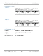
AP231 Model 


AD5761 @ -40oC to 85oC: 

Linearity Error is +/- 0.003% FSR maximum (i.e. +/-2 LSB). 

Offset Error is +/- 0.05% FSR (i.e. 20V SPAN) maximum.   

Gain Error is +/- 0.1% FSR maximum. 

Total Error 

+/- 0.153% FSR maximum (+/-98.5 LSB)


AP220 Model 


AD5721 @ -40oC to 85oC: 

Linearity Error is +/- 0.0122% FSR maximum (i.e. +/-0.5 LSB). 

Offset Error is +/- 0.05% FSR (i.e. 20V SPAN) maximum. 

Gain Error is +/- 0.1% FSR maximum. 

Total Error 

+/- 0.1622% FSR maximum (+/-6.64 LSB)


Typically, each error component is much less than its maximum and all error 
components do not reinforce each other.  Thus, typical errors are much less 
than that shown above.


Summary of Contents for AP220 AcroPack

Page 1: ...gh Density Analog Output Module USER S MANUAL ACROMAG INCORPORATED 30765 South Wixom Road Wixom MI 48393 2417 U S A Tel 248 295 0310 Email solutions acromag com Copyright 2016 Acromag Inc Printed in the USA Data and specifications are subject to change without notice 8501059G ...

Page 2: ...tion All Models 4 1 3 1 Ordering Information 5 1 3 2 Key Features 5 1 3 3 Key Features PCIe Interface 6 1 4 Signal Interface Products 6 1 5 Software Support 6 Windows 7 VxWorks 7 Linux 7 1 6 References 7 2 0 PREPARATION FOR USE 8 2 1 Unpacking and Inspecting 8 2 2 Installation Considerations 9 2 3 Non Isolation Considerations 9 2 4 Default Hardware Configuration 9 2 5 Programmable Register Configu...

Page 3: ...Transparent Mode 21 Simultaneous Mode Read Write BAR0 0x0000 0048 21 Simultaneous Output Trigger Write Only BAR0 0x0000 004C 21 DAC Write Status Register Read Only BAR0 0x0000 0054 22 Control Register Write Only BAR0 0x0000 0058 22 XADC Status Control Register Read Write BAR0 0x0000 0088 23 XADC Address Register Write Only BAR0 0x0000 008C 23 Table 3 7 System Monitor Register Map 24 Firmware Revis...

Page 4: ...S 32 6 1 Physical 32 6 2 Power Requirements 33 6 3 Environmental Considerations 33 6 3 1 Operating Temperature 33 6 3 2 Other Environmental Requirements 34 6 3 2 1 Relative Humidity 34 6 3 2 2 Isolation 34 6 3 3 Vibration and Shock Standards 34 6 3 4 EMC Directives 34 6 4 Reliability Prediction 35 AP220 16E 35 AP231 16E 35 6 5 PCIe Bus Specifications 35 Table 6 5 PCIe Bus Data Rates 36 APPENDIX 37...

Page 5: ... or reproduced in any form without the prior written consent of Acromag 1 2 1 Trademark Trade Name and Copyright Information 2016 by Acromag Incorporated All rights reserved Acromag and Xembedded are registered trademarks of Acromag Incorporated All other trademarks registered trademarks trade names and service marks are the property of their respective owners 1 2 2 Class A Product Warning This is...

Page 6: ...2 Bit Analog Output 40 C to 85 C AP231 16E LF1 16 Channel 16 Bit Analog Output 40 C to 85 C Note 1 Applications requiring operating temperatures of 70 C to 85 C will require purchase of AcroPack Heatsink Accessory AP CC 01 and minimum airflow of 400LFM For temperatures below 70 C the module will require a minimal airflow of 200LFM AP CC 01 AcroPack Conduction Cool Kit See Appendix for installation...

Page 7: ...puts reset to 0 volts following a power up or reset Alarm Software readable monitor Brownout short circuit and Die temperature 150C 1 3 3 Key Features PCIe Interface PCIe Bus The AP module includes a PCI Express Generation 1 interface operating at a bus speed of 2 5 Gbps with one lane in each direction Compatibility PCI Express Base Specification v2 1 compliant PCI Express Endpoint 1 4 Signal Inte...

Page 8: ...ware This software Model APSW API VXW is composed of VxWorks real time operating system libraries for all AcroPack modules VPX I O board products and PCIe I O Cards The software is implemented as a library of C functions which link with existing user code to make possible simple control of all Acromag AcroPack modules Linux Acromag provides a software product consisting of Linux software This soft...

Page 9: ...this product near strong electrostatic electromagnetic magnetic or radioactive fields unless the device is contained within its original manufacturer s packaging Be aware that failure to comply with these guidelines will void the Acromag Limited Warranty 2 1 Unpacking and Inspecting Upon receipt of this product inspect the shipping carton for evidence of mishandling during transit If the shipping ...

Page 10: ...iltering In a conduction cooled assembly adequate thermal conduction must be provided to prevent a temperature rise above the maximum operating temperature 2 3 Non Isolation Considerations The board is non isolated since there is electrical continuity between the PCIe bus and AcroPack module grounds As such the field I O connections are not isolated from the system Care should be taken in designin...

Page 11: ...SERIES AP220 AP231 ACROPACK USER S MANUAL Acromag Inc Tel 248 295 0310 10 http www acromag com 10 https www acromag com 2 6 Functional Block diagram ...

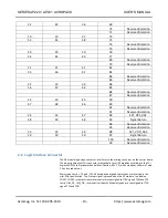
Page 12: ...ts signal pin assignments for the module field I O connector Every other pin of the 100 pin connector is left unconnected in order to meet the minimum distance required for 60 Volt isolation Table 2 1 Field I O Connector Pin Assignments 68 Pin Champ Carrier Connector 50 Pin Champ Carrier Connector2 Ribbon Carrier Connector1 Module P2 Pin Number Field I O Signal 1 1 1 2 CH0 35 26 2 1 Signal Return ...

Page 13: ...39 Reserved isolation 11 11 21 42 CH10 45 36 22 41 Signal Return 44 Reserved isolation 43 Reserved isolation 12 12 23 46 CH11 46 37 24 45 Signal Return 48 Reserved isolation 47 Reserved isolation 13 13 25 50 CH12 47 38 26 49 Signal Return 52 Reserved isolation 51 Reserved isolation 14 14 27 54 CH13 48 39 28 53 Signal Return 56 Reserved isolation 55 Reserved isolation 15 15 29 58 CH14 49 40 30 57 S...

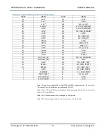
Page 14: ...5 Reserved isolation 25 25 49 98 EXT_VDD_DAC 59 50 50 97 Signal Return 100 Reserved isolation 99 Reserved isolation 2 8 Logic Interface Connector The AP module logic edge connector interfaces to the mating connector on the carrier board The pin assignments of this connector are standard for all AP modules according to the PCI Express MINI Card Electromechanical Specification REV 1 2 with exception...

Page 15: ...0 26 GND 23 PERn0 24 3 3V3 21 GND 22 PERST 19 TDI UIM_C4 1 20 N C W_DISABLE 1 17 TDO UIM_C8 1 18 GND 15 GND 16 N C UIM_VPP 1 13 RECLK 14 N C UIM_RESET 1 11 REFCLK 12 N C UIM_CLK 1 9 GND 10 N C UIM_DATA 1 7 CLKREQ 8 N C UIM_PWR 1 5 TCK COEX2 1 6 N C 1 5V 1 3 TMS COEX1 1 4 GND 1 N C WAKE 1 2 3 3V3 Note 1 Signals are not applicable for the AP220 and AP231 implementation Pins are either no connects on...

Page 16: ... the PCIe card The system software accesses the configuration registers to determine how many blocks of memory space the module requires It then programs the board s configuration registers with the unique memory base address Since this board is not fixed in address space its device driver must use the mapping information stored in the board s Configuration Space registers to determine where the b...

Page 17: ...to access the PCIe interrupt and I O registers The PCIe bus decodes 4K bytes for BAR0 for this memory space The memory space address map for the AP220 or AP231 is shown in Table 3 2 Note that the base address for the board BAR0 in memory space must be added to the addresses shown to properly access these AP220 and AP231 registers Register accesses as 32 16 and 8 bit data in memory space are permit...

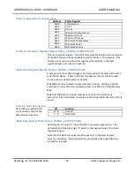
Page 18: ...1 0 DAC Channel 14 0x0000 0044 31 0 DAC Channel 15 0x0000 0048 31 0 Simultaneous Mode 0x0000 004C 31 0 Simultaneous Output Trigger 0x0000 0050 31 0 Not Used 0x0000 0054 31 0 DAC Write Status 0x0000 0058 31 0 DAC Reset Control 0x0000 005C 0x00000084 31 0 Not Used 0x0000 0088 XADC Status Control Register 0x0000 008C XADC Address Register 0x0000 0090 0x000001FC Not Used 0x0000 0200 31 0 Firmware Revi...

Page 19: ...quires write of two read commands to complete serial shift out of the DAC data or control value Then read the DAC channel register will contain the read data in the lower 16 bits for AP231 and bits 15 to 4 of the AP220 See Table 3 5 for the allowed DAC write and read commands The contents of the DAC Channel registers are transferred to their corresponding converter input buffer serially This seria...

Page 20: ...ssue of two commands and 1 6µs 1011 Readback DAC register Provides contents of DAC register after issue of two commands and 1 6µs 1100 Readback control register Provides contents of control register after issue of two commands and 1 6µs See Table 3 6 for description of DAC Control register 1101 No operation 1110 No operation 1111 Software full reset Device set to power up state output at AGND and ...

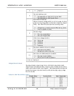
Page 21: ...9 2 bits Clear voltage selection 00 Zero scale 01 Midscale 10 Full scale 11 Full scale 11 Brownout condition status on readback 0 No brownout condition 1 Brownout condition detected 12 Short circuit condition status on readback 0 No short circuit condition 1 Short circuit condition detected 15 to 13 Not Used Output Data Format The default bipolar output range 10 to 10 Volts is programmed with stra...

Page 22: ... 0 set to logic 1 in order to select Simultaneous Mode RESET CONDITION Defaults to Simultaneous Mode All analog output channels are set to 0 Volts Note The reset function resets only the DAC output latch of the input double buffer Therefore after a reset good data must be written using Write to input register DAC Command 0001 to all the input latches before enabling the Simultaneous Output Trigger...

Page 23: ...hannel register can be performed no sooner than 1 6µs after the previous DAC write command is executed The status of 16 DAC channels numbered 0 through 15 may be monitored via this register Data bits 0 to 15 reflect the status of DAC channels 0 to 15 The channels corresponding status bit will be set low upon initiation of a write operation and will remain low until the requested write operation ha...

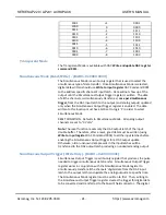
Page 24: ...one of the table below Reading or writing this register is possible via 32 bit data transfers The 10 bits digitized and output from the ADC can be converted to temperature by using the following equation 15 273 1024 975 503 ADCcode C e Temperatur The 10 bits digitized and output from the ADC can be converted to voltage by using the following equation V ADCcode volts age SupplyVolt 3 1024 XADC Addr...

Page 25: ...l transfer to from the serial FLASH device A byte read from this address returns the data read from a previous write read serial transfer WARNING Factory calibration data is stored in FLASH Writing to FLASH could result in loss of factory calibration data See Table 3 7 Flash Memory Map Note that the Flash chip select must be set prior to the start of any instruction Flash chip select must also be ...

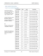
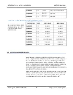
Page 26: ...GainCoef LSB 0x3F E003 7 0 10 to 10V Channel 0 GainCoef MSB 0x3F E004 7 0 0 to 10V Channel 0 OffsetCoef LSB 0x3F E005 7 0 0 to 10V Channel 0 OffsetCoef MSB 0x3F E006 7 0 0 to 10V Channel 0 GainCoef LSB 0x3F E007 7 0 0 to 10V Channel 0 GainCoef MSB 0x3F E008 7 0 5 to 5V Channel 0 OffsetCoef LSB 0x3F E009 7 0 5 to 5V Channel 0 OffsetCoef MSB 0x3F E00A 7 0 5 to 5V Channel 0 GainCoef LSB 0x3F E00B 7 0...

Page 27: ...Reserved Reserved 4 0 USE OF CALIBRATION DATA Calibration data is provided in the form of calibration coefficients so the user can adjust and improve the accuracy of the analog output voltage over the uncalibrated state Each channel s unique offset and gain calibration coefficients are stored in Flash memory The use of software calibration allows the elimination of hardware calibration potentiomet...

Page 28: ...ibrated errors observed may be much less The maximum uncalibrated error is summarized as follows AP231 Model AD5761 40oC to 85oC Linearity Error is 0 003 FSR maximum i e 2 LSB Offset Error is 0 05 FSR i e 20V SPAN maximum Gain Error is 0 1 FSR maximum Total Error 0 153 FSR maximum 98 5 LSB AP220 Model AD5721 40oC to 85oC Linearity Error is 0 0122 FSR maximum i e 0 5 LSB Offset Error is 0 05 FSR i ...

Page 29: ...ing the linearity and adjusted offset and gain errors AP231 Model AD5761 40oC to 85oC Linearity Error is 2 LSB Offset Error is 0 0625 LSB Gain Error is 0 0625 LSB Total Error 2 125 LSB 0 0032 FSR maximum AP220 Model AD5721 40oC to 85oC Linearity Error is 0 5 LSB Offset Error is 0 0625 LSB Gain Error is 0 0625 LSB Total Error 0 625 LSB 0 0152 FSR maximum Thus correcting the value programmed to the ...

Page 30: ...0 to 10V 204 8 2048 0 5 to 5V 409 6 2048 0 3 to 3V 682 6 2048 0 2 5 to 7 5V 409 6 1024 1024 0 to 10V 409 6 0 2048 0 to 5V 819 2 0 2048 Using equation 1 one can determine the IdealCode for any desired voltage within the range For example if it is desired to output a voltage of 5 Volts for 10 to 10V range equation 1 returns the result 49 152 for IdealCode for Model AP231 If this value is used to pro...

Page 31: ... are stored as 2 s complement to allow of plus and minus values AP231 Model GainCoef 65536 16 𝐴𝑐𝑡𝑢𝑎𝑙𝑆𝑙𝑜𝑝𝑒 𝐼𝑑𝑒𝑎𝑙𝑆𝑙𝑜𝑝𝑒 1 OffsetCoef ActualZeroCode IdealZeroCode 16 ActualSlope 𝐶𝑜𝑑𝑒2 𝐶𝑜𝑑𝑒1 𝑀𝑒𝑎𝑠𝑢𝑟𝑒𝑑𝑉2 𝑀𝑒𝑎𝑠𝑢𝑟𝑒𝑑𝑉1 ActualZeroCode Code1 ActualSlope 𝑀𝑒𝑎𝑠𝑢𝑟𝑒𝑑𝑉1 Where Code1 655 0x28F hex Code2 64880 0xFD70 hex Measured values 𝑀𝑒𝑎𝑠𝑢𝑟𝑒𝑑𝑉2 𝑎𝑛𝑑 𝑀𝑒𝑎𝑠𝑢𝑟𝑒𝑑𝑉1 are taken using data averaging Equation 3 AP220 Model Cor...

Page 32: ...TURNED OFF BEFORE SERVICING BOARDS Before beginning repair be sure that all of the procedures in the Preparation for Use section have been followed Also refer to the documentation of your carrier board to verify that it is correctly configured Replacement of the board with one that is known to work correctly is a good technique for isolating a faulty part 5 3 Where to Get Help If you continue to h...

Page 33: ...2 https www acromag com 6 0 SPECIFICATIONS 6 1 Physical Height 12 5 mm 0 4921 in Height defines Carrier to Module Maximum component height Board Thickness 1 0 mm 0 03937 in AcroPack L x W 70 mm x 30 00 mm 2 76 in x 1 18 in Unit Weight does not include shipping material AcroPack 0 016 lbs 0 0074 kg ...

Page 34: ...um airflow of 400LFM For temperatures below 70 C the module will require a minimum airflow of 200LFM AP CC 01 AcroPack Conduction Cool Kit See Appendix for installation instructions Summarized below are the expected current draws for each of the specified power supply voltages The current draw is the same for both AP220E and AP231E Power Supply Voltage Current Draw 3 3 VDC 5 1 400 mA Typical 480 m...

Page 35: ...ory 20 Ground vehicles ground mobile 8 500Hz Sinusoidal 5Grms X Y and Z axis 1hr per axis 15 minute sweep up 15 minute sweep down test duration Shock Operating MIL STD 810G Method 516 6 Procedure I functional Shock 50g 11ms half sine 3 positive negative per axis Total of 18 drops 6 3 4 EMC Directives The AcroPack is designed to comply with EMC Directive 2004 108 EC Immunity per EN 61000 6 2 Electr...

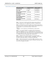
Page 36: ... 9 40 C 792 959 90 5 1 261 1 1 FIT is Failures in 109 hours AP231 16E MTBF Mean Time Between Failure MTBF in hours using MIL HDBK 217F FN2 Per MIL HDBK 217 Ground Benign Controlled GBGC Temperature MTBF Hours MTBF Years Failure Rate FIT1 25 C 2 190 883 250 1 456 4 40 C 1 241 382 141 7 805 6 1 FIT is Failures in 109 hours 6 5 PCIe Bus Specifications Compatibility Conforms to PCI Express Base Specif...

Page 37: ...is 20 Bytes with data payload of 4 Bytes for our typical AcroPack For each 4 Byte data sample 24 Bytes are sent 250𝑀𝐵𝑦𝑡𝑒 𝑠 24 𝐵𝑦𝑡𝑒𝑠 10 4 M samples sec or 41 6 M Bytes sec or 0 332 G bit sec Note 3 For our typical AcroPack have measured back to back 4 Byte read operations completing every 1 7usec A read operation starts with a host read request The AcroPack must process the read and fetch the data ...

Page 38: ...c Tel 248 295 0310 37 http www acromag com 37 https www acromag com Appendix AP CC 01 Heatsink Kit Installation This example will show how to install the AP CC 01 Heatsink kit with an APCe7020 carrier AP CC 01 Heat Sink Kit Bottom view Top view Hardware ...

Page 39: ...CK USER S MANUAL Acromag Inc Tel 248 295 0310 38 http www acromag com 38 https www acromag com 1 Install two standoffs and secure with two screws 2 Install the AcroPack module 3 Install the Heatsink and secure with 4 screws 1 2 ...

Page 40: ...20 AP231 ACROPACK USER S MANUAL Acromag Inc Tel 248 295 0310 39 http www acromag com 39 https www acromag com 4 AP CC 01 Installation is complete Note Make sure the thermal pad is making contact with the FPGA IC ...

Page 41: ...difiable Yes No Function FPGA logic blocks Process to Sanitize Power Down Type SRAM SDRAM etc Size User Modifiable Yes No Function Process to Sanitize Non Volatile Memory Does this product contain Non Volatile memory i e Memory of whose contents is retained when power is removed Yes No Type EEPROM Flash etc Size 32 Meg x 1bit User Modifiable Yes No Function Data storage for FPGA Process to Sanitiz...

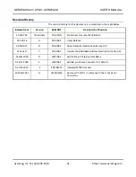
Page 42: ...MAY 16 Preliminary PDG PDG Preliminary Document Publication 29 JUN 16 A PDG ARP Initial Release 09 MAR 17 B PDG ARP Added module location feature sec 3 3 21 Sept 17 C PDG ARP Update the BAR0 Base Address Description Table 3 2 16 JAN 2018 D LMP ARP Add Table 6 5 PCIe Bus Data Rates 03 JULY 2018 E LMP ARP Add 68 pin Champ Connector to Table 2 1 04 DEC 2020 F ENZ AMM Updated MTBF Numbers 10 MAR 2021 ...

Reviews: