AcroPack Series APCe7012E-LF
PCI Express Carrier Board
- 16 -
is on the top (component) side of the carrier board while “A” is on the bottom
(solder) side. Connector “gold finger” numbers increase with distance from
the bracket end of the printed circuit board.
Refer to the PCI Express bus specification for additional information on the
PCI Express bus signals.
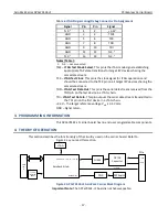
Table 5 PCIe Bus P1 CONNECTIONS
Signal
Pin
Pin
Signal
+12V
B01
A01
PRSNT1*
+12V
B02
A02
+12V
+12V
B03
A03
+12V
GND
B04
A04
GND
SMCLK
B05
A05
TCK
SMDAT
B06
A06
TDI
GND
B07
A07
TDO
+3.3V
B08
A08
TMS
TRST*
B09
A09
+3.3V
+3.3Vaux
3
B10
A10
+3.3V
WAKE*
B11
A11
PERST*
RSVD
B12
A12
GND
GND
B13
A13
REFCLKp
Tx0p
B14
A14
REFCLKn
Tx0n
B15
A15
GND
GND
B16
A16
Rx0p
N.C.
B17
A17
Rx0n
GND
B18
A18
GND
Notes (Table ):
1.
Asterisk (*) is used to indicate an active-low signal.
2.
BOLD ITALIC Logic Lines are NOT USED by the carrier board.
3.
+3.3Vaux power to AcroPack is not used by the carrier. Contact Acromag to
3.3Vaux power to the AcroPack module. The carrier pr3.3V
power to the module.
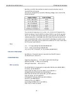
JTAG Programming/Debug Connector
A JTAG programming/debug connector is provided for developing applications
that use Acromag’s FPGA AcroPack modules. See reference designator P3 in
Error! Reference source not found.
. This is a standard 14-pin Xilinx
programming header for connecting a Xilinx Platform USB II programming
device (or equivalent). The pin assignment for P3 is shown in Table . A CPLD
on the carrier is included in the JTAG chain. The Xilinx Vivado tools can detect
the presence of the CPLD in the JTAG chain and skip it when accessing the
FPGAs on the AcroPack modules.


