AcroPack Series APCe7012E-LF
PCI Express Carrier Board
- 17 -
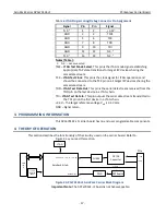
Table 6 JTAG Programming/Debug Connector Pin Assignment
Signal
Pin
Pin
Signal
N.C.
1
1
2
_+3.3V
GND
3
4
TMS
GND
5
6
TCK
GND
7
8
TDO
GND
9
10
TDI
GND
11
12
N.C.
1
N.C.
1
13
14
N.C.
1
Notes (Table ):
1.
N.C. – not connected
TMS –
JTAG Test Mode Select
. This pin is the JTAG mode signal establishing
appropriate TAP state transitions for target ISP devices sharing the
same data stream.
TCK –
JTAG Test Clock
. This pin is the clock signal for JTAG operations and
should be connected to the TCK pin on all target ISP devices sharing the
same data stream.
TDO –
JTAG Test Data Out
. This pin is the serial data stream received from the
TDO pin on the last device in a JTAG chain.
TDI –
JTAG Test Data In
. This pin outputs the serial data stream transmitted to
the TDI pin on the first device in a JTAG chain.
+3.3V – The target reference voltage V
REF
is 3.3 Volts.
GND – Signal return.
3.
PROGRAMMING INFORMATION
This APCe7012E-LF carrier board has no end user programmable components.
4.
THEORY OF OPERATION
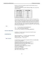
This section describes the functionality of the circuitry used on the carrier board. Refer to
Figure 3 as you read this section.
+3.3V
+12V
PCIe
Field
I/O
A
AcroPack Site A
x1 PCIe
DC/DC
Converter
FUSES
Power +1.5, +3.3, +5, +12, -12
JTAG
CPLD
DIP Switch
Slot Address
+/- 12 V
Isolated
Power
+/- 12 V
Isolated
Power
Figure 3 APCe7012E-LF AcroPack Carrier Block Diagram
Important Note:
The APCe7012E-LF board is not hot-swappable.


